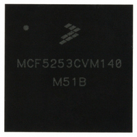
MCF5253CVM140 Freescale Semiconductor, MCF5253CVM140 Datasheet - Page 54

MCF5253CVM140
Manufacturer Part Number
MCF5253CVM140
Description
IC MPU 32BIT 140MHZ 225-MAPBGA
Manufacturer
Freescale Semiconductor
Series
MCF525xr
Datasheets
1.MCF5253VM140J.pdf
(34 pages)
2.MCF5253VM140J.pdf
(8 pages)
3.MCF5253VM140J.pdf
(648 pages)
4.MCF5253VM140J.pdf
(2 pages)
Specifications of MCF5253CVM140
Core Processor
Coldfire V2
Core Size
32-Bit
Speed
140MHz
Connectivity
CAN, EBI/EMI, I²C, QSPI, UART/USART, USB OTG
Peripherals
DMA, WDT
Program Memory Type
ROMless
Ram Size
128K x 8
Voltage - Supply (vcc/vdd)
1.08 V ~ 1.32 V
Data Converters
A/D 6x12b
Oscillator Type
External
Operating Temperature
-40°C ~ 85°C
Package / Case
225-MAPBGA
Family Name
MCF5xxx
Device Core
ColdFire V2
Device Core Size
32b
Frequency (max)
140MHz
Instruction Set Architecture
RISC
Supply Voltage 1 (typ)
1.2/3.3V
Operating Supply Voltage (max)
1.32/3.6V
Operating Supply Voltage (min)
1.08/3V
Operating Temp Range
-40C to 85C
Operating Temperature Classification
Industrial
Mounting
Surface Mount
Pin Count
225
Package Type
MA-BGA
Lead Free Status / RoHS Status
Lead free / RoHS Compliant
Number Of I /o
-
Eeprom Size
-
Program Memory Size
-
Lead Free Status / Rohs Status
Compliant
Available stocks
Company
Part Number
Manufacturer
Quantity
Price
Company:
Part Number:
MCF5253CVM140
Manufacturer:
FREESCALE
Quantity:
300
Company:
Part Number:
MCF5253CVM140
Manufacturer:
Freescale Semiconductor
Quantity:
10 000
Part Number:
MCF5253CVM140
Manufacturer:
FREESCALE
Quantity:
20 000
Company:
Part Number:
MCF5253CVM140J
Manufacturer:
Freescale Semiconductor
Quantity:
10 000
- MCF5253VM140J PDF datasheet
- MCF5253VM140J PDF datasheet #2
- MCF5253VM140J PDF datasheet #3
- MCF5253VM140J PDF datasheet #4
- Current page: 54 of 648
- Download datasheet (8Mb)
Signal Description
2.9
The following signals transfer serial data between the three UART modules and external peripherals.
2.10
The following signal provides an external interface to Timer0. One 16-bit timers can trigger external
events or both 16-bit timers can trigger internal interrupts.
2.11
The following signals provide the external audio interface.
2-8
I
Serial Module Signal
2
I
c Module Signal
I
2
2
Request To Send
C Serial Clock
C Serial Data
Clear To Send
Transmit Data
Receive Data
Timer Signal
Timer Output
Serial Module Signals
Timer Module Signals
Serial Audio Interface Signals
The SCL0/SDATA1_BS1/GPIO41, and SCL1/TXD1/GPIO10 bidirectional signals are the clock signal for
first and second I
all I
Signals are multiplexed.
The SDA0/SDATA3/GPIO42 and SDA1/RXD1/GPIO44 bidirectional signals are the data input/output for
the first and second serial I
Signals are multiplexed.
The RXD0/GPIO46, SDA1/RXD1/GPIO44, and EF/RXD2/GPIO6 are the inputs on which serial data is
The UART transmits serial data on the TXD0/GPIO45, SCL1/TXD1/GPIO10, and XTRIM/TXD2/GPIO0
received by the UART. Data is sampled on RxD[2:0] on the rising edge of the serial clock source, with
the least significant bit received first.
output signals. Data is transmitted on the falling edge of the serial clock source, with the least significant
bit transmitted (LSB) first. When no data is being transmitted or the transmitter is disabled, these two
signals are held high. TxD[2:0] are also held high in local loopback mode.
The DDATA3/RTS0/GPOI4 and DDATA1/RTS1/SDATA2_BS2/GPIO2 request-to-send outputs indicate
to the peripheral device that UART0/1 are ready to send data and requires a clear-to-send signal to
initiate transfer. The third UART lacks flow control using RTS/CTS.
Peripherals drive the DDATA2/CTS0/GPIO3 and DDATA0/CTS1/SDATA0_SDIO1/GPIO1 inputs to
indicate to the MCF5253 serial module that it can begin data transmission. The third UART lacks flow
control using RTS/CTS.
2
The SDATAO1/TOUT0/GPIO18 programmable output pulse or toggle on various timer events.
C devices drive this signal to synchronize I
2
C module operation. The I
Table 2-4. Serial Module Signals
Table 2-5. Timer Module Signals
MCF5253 Reference Manual, Rev. 1
Table 2-3. I
2
C interface.
2
C Module Signals
2
C module controls this signal when the bus is in master mode;
Description
2
Description
Description
C timing.
Freescale Semiconductor
Related parts for MCF5253CVM140
Image
Part Number
Description
Manufacturer
Datasheet
Request
R
Part Number:
Description:
Mcf5253 Coldfire? Microprocessor Data Sheet
Manufacturer:
Freescale Semiconductor, Inc
Datasheet:
Part Number:
Description:
Manufacturer:
Freescale Semiconductor, Inc
Datasheet:
Part Number:
Description:
Manufacturer:
Freescale Semiconductor, Inc
Datasheet:
Part Number:
Description:
Manufacturer:
Freescale Semiconductor, Inc
Datasheet:
Part Number:
Description:
Manufacturer:
Freescale Semiconductor, Inc
Datasheet:
Part Number:
Description:
Manufacturer:
Freescale Semiconductor, Inc
Datasheet:
Part Number:
Description:
Manufacturer:
Freescale Semiconductor, Inc
Datasheet:
Part Number:
Description:
Manufacturer:
Freescale Semiconductor, Inc
Datasheet:
Part Number:
Description:
Manufacturer:
Freescale Semiconductor, Inc
Datasheet:
Part Number:
Description:
Manufacturer:
Freescale Semiconductor, Inc
Datasheet:
Part Number:
Description:
Manufacturer:
Freescale Semiconductor, Inc
Datasheet:
Part Number:
Description:
Manufacturer:
Freescale Semiconductor, Inc
Datasheet:
Part Number:
Description:
Manufacturer:
Freescale Semiconductor, Inc
Datasheet:
Part Number:
Description:
Manufacturer:
Freescale Semiconductor, Inc
Datasheet:
Part Number:
Description:
Manufacturer:
Freescale Semiconductor, Inc
Datasheet:


