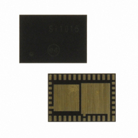
SI1011-A-GM Silicon Laboratories Inc, SI1011-A-GM Datasheet - Page 180

SI1011-A-GM
Manufacturer Part Number
SI1011-A-GM
Description
IC TXRX MCU + EZRADIOPRO
Manufacturer
Silicon Laboratories Inc
Specifications of SI1011-A-GM
Package / Case
42-QFN
Frequency
240MHz ~ 960MHz
Data Rate - Maximum
256kbps
Modulation Or Protocol
FSK, GFSK, OOK
Applications
General Purpose
Power - Output
20dBm
Sensitivity
-121dBm
Voltage - Supply
1.8 V ~ 3.6 V
Current - Receiving
18.5mA
Current - Transmitting
85mA
Data Interface
PCB, Surface Mount
Memory Size
8kB Flash, 768B RAM
Antenna Connector
PCB, Surface Mount
Number Of Receivers
1
Number Of Transmitters
1
Wireless Frequency
240 MHz to 960 MHz
Interface Type
UART, SMBus, SPI, PCA
Output Power
20 dBm
Operating Supply Voltage
0.9 V to 3.6 V
Maximum Operating Temperature
+ 85 C
Mounting Style
SMD/SMT
Maximum Supply Current
4 mA
Minimum Operating Temperature
- 40 C
Modulation
FSK, GFSK, OOK
Protocol Supported
C2, SMBus
Core
8051
Program Memory Type
Flash
Program Memory Size
8 KB
Data Ram Size
768 B
Supply Current (max)
4 mA
Lead Free Status / RoHS Status
Lead free / RoHS Compliant
Operating Temperature
-
Lead Free Status / Rohs Status
Lead free / RoHS Compliant
Other names
336-1872-5
Available stocks
Company
Part Number
Manufacturer
Quantity
Price
Company:
Part Number:
SI1011-A-GM
Manufacturer:
Silicon Laboratories Inc
Quantity:
135
- Current page: 180 of 384
- Download datasheet (3Mb)
Si1010/1/2/3/4/5
16.10. Low Power Mode
Setting the LPEN bit in the DC0CF register will enable a Low Power Mode for the dc-dc converter. In Low
Power Mode, the bias currents are substantially reduced, which can lead to an efficiency improvement with
light load currents (generally less than a few mA). The drawback to this mode is that the response time of
the converter’s analog blocks is increased; larger delay in the circuits controlling the Diode Bypass switch
can lead to loss of efficiency at medium and high load currents due to reverse leakage in the switch. The
Low power mode also reduces the peak inductor current limit as shown in Table 16.1.
16.11. Passive Diode Mode
Setting the EXTDEN bit in DC0MD enables the Passive Diode Mode. In this mode, the control circuits for
the Diode Bypass switch are disabled, which reduces the converter’s quiescent operating current. An
external Schottky diode may be connected between the DCEN (anode) and VDD_MCU/DC+ (cathode)
pins. Under light load conditions, an external diode is typically not required. There are two situations in
which this mode can prove beneficial. First is with very light load currents, where the efficiency is domi-
nated by the converter’s quiescent current. The converter will use an internal p-n junction diode to transfer
current from the inductor to the output capacitor; although there is a larger voltage drop (and power loss)
across a passive diode, the overall efficiency may be improved due to the reduction in quiescent current.
The second situation is when output power is very high. In that case, efficiency can suffer because some
reverse current can flow in the Diode Bypass switch before the control circuitry turns the switch off. Putting
the device in Passive Diode Mode and optionally connecting an external Schottky diode between the
DCEN and VDD_MCU/DC+ pins (parallel to the internal diode) may provide higher efficiency in some
applications than using the internal Diode Bypass switch.
180
Rev. 1.0
Related parts for SI1011-A-GM
Image
Part Number
Description
Manufacturer
Datasheet
Request
R
Part Number:
Description:
QFN 42/I�/8KB, 768B RAM, +20 DBM, PROGRAMMABLE XCVR
Manufacturer:
Silicon Laboratories Inc
Part Number:
Description:
SMD/C�/SINGLE-ENDED OUTPUT SILICON OSCILLATOR
Manufacturer:
Silicon Laboratories Inc
Part Number:
Description:
Manufacturer:
Silicon Laboratories Inc
Datasheet:
Part Number:
Description:
N/A N/A/SI4010 AES KEYFOB DEMO WITH LCD RX
Manufacturer:
Silicon Laboratories Inc
Datasheet:
Part Number:
Description:
N/A N/A/SI4010 SIMPLIFIED KEY FOB DEMO WITH LED RX
Manufacturer:
Silicon Laboratories Inc
Datasheet:
Part Number:
Description:
N/A/-40 TO 85 OC/EZLINK MODULE; F930/4432 HIGH BAND (REV E/B1)
Manufacturer:
Silicon Laboratories Inc
Part Number:
Description:
EZLink Module; F930/4432 Low Band (rev e/B1)
Manufacturer:
Silicon Laboratories Inc
Part Number:
Description:
I�/4460 10 DBM RADIO TEST CARD 434 MHZ
Manufacturer:
Silicon Laboratories Inc
Part Number:
Description:
I�/4461 14 DBM RADIO TEST CARD 868 MHZ
Manufacturer:
Silicon Laboratories Inc
Part Number:
Description:
I�/4463 20 DBM RFSWITCH RADIO TEST CARD 460 MHZ
Manufacturer:
Silicon Laboratories Inc
Part Number:
Description:
I�/4463 20 DBM RADIO TEST CARD 868 MHZ
Manufacturer:
Silicon Laboratories Inc
Part Number:
Description:
I�/4463 27 DBM RADIO TEST CARD 868 MHZ
Manufacturer:
Silicon Laboratories Inc
Part Number:
Description:
I�/4463 SKYWORKS 30 DBM RADIO TEST CARD 915 MHZ
Manufacturer:
Silicon Laboratories Inc
Part Number:
Description:
N/A N/A/-40 TO 85 OC/4463 RFMD 30 DBM RADIO TEST CARD 915 MHZ
Manufacturer:
Silicon Laboratories Inc


