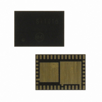
SI1011-A-GM Silicon Laboratories Inc, SI1011-A-GM Datasheet - Page 99

SI1011-A-GM
Manufacturer Part Number
SI1011-A-GM
Description
IC TXRX MCU + EZRADIOPRO
Manufacturer
Silicon Laboratories Inc
Specifications of SI1011-A-GM
Package / Case
42-QFN
Frequency
240MHz ~ 960MHz
Data Rate - Maximum
256kbps
Modulation Or Protocol
FSK, GFSK, OOK
Applications
General Purpose
Power - Output
20dBm
Sensitivity
-121dBm
Voltage - Supply
1.8 V ~ 3.6 V
Current - Receiving
18.5mA
Current - Transmitting
85mA
Data Interface
PCB, Surface Mount
Memory Size
8kB Flash, 768B RAM
Antenna Connector
PCB, Surface Mount
Number Of Receivers
1
Number Of Transmitters
1
Wireless Frequency
240 MHz to 960 MHz
Interface Type
UART, SMBus, SPI, PCA
Output Power
20 dBm
Operating Supply Voltage
0.9 V to 3.6 V
Maximum Operating Temperature
+ 85 C
Mounting Style
SMD/SMT
Maximum Supply Current
4 mA
Minimum Operating Temperature
- 40 C
Modulation
FSK, GFSK, OOK
Protocol Supported
C2, SMBus
Core
8051
Program Memory Type
Flash
Program Memory Size
8 KB
Data Ram Size
768 B
Supply Current (max)
4 mA
Lead Free Status / RoHS Status
Lead free / RoHS Compliant
Operating Temperature
-
Lead Free Status / Rohs Status
Lead free / RoHS Compliant
Other names
336-1872-5
Available stocks
Company
Part Number
Manufacturer
Quantity
Price
Company:
Part Number:
SI1011-A-GM
Manufacturer:
Silicon Laboratories Inc
Quantity:
135
- Current page: 99 of 384
- Download datasheet (3Mb)
5.9. Voltage and Ground Reference Options
The voltage reference MUX is configurable to use an externally connected voltage reference, one of two
internal voltage references, or one of two power supply voltages (see Figure 5.10). The ground reference
MUX allows the ground reference for ADC0 to be selected between the ground pin (GND) or a port pin
dedicated to analog ground (P0.1/AGND).
The voltage and ground reference options are configured using the REF0CN SFR described on page 101.
Electrical specifications are can be found in the Electrical Specifications Chapter.
Important Note About the V
inputs. When using an external voltage reference or the internal precision reference, P0.0/VREF should be
configured as an analog input and skipped by the Digital Crossbar. When using AGND as the ground refer-
ence to ADC0, P0.1/AGND should be configured as an analog input and skipped by the Digital Crossbar.
Refer to Section “21. Port Input/Output” on page 219 for complete Port I/O configuration details. The exter-
nal reference voltage must be within the range 0 V
ence must be at the same DC voltage potential as GND.
4 .7 F
B ypass C apacitors
R ecom m ended
G N D
V D D
+
R 1
R eference
E xternal
V oltage
C ircuit
0 .1 F
Figure 5.10. Voltage Reference Functional Block Diagram
V D D _M C U /D C +
P 0.1/A G N D
P 0.0/V R E F
REF
G N D
and AGND Inputs: Port pins are used as the external V
Internal 1.68V
R E F O E
R eference
E N
Rev. 1.0
R egulated D igital S upply
H igh S peed R eference
R E F 0C N
REF
Internal 1.65 V
Internal 1.8V
VDD_MCU/DC+ and the external ground refer-
Si1010/1/2/3/4/5
E N
T em p S ensor
R E F G N D
00
01
10
11
0
1
REF
and AGND
(to A D C )
(to A D C )
V R E F
G round
Input
A D C
M ux
99
Related parts for SI1011-A-GM
Image
Part Number
Description
Manufacturer
Datasheet
Request
R
Part Number:
Description:
QFN 42/I�/8KB, 768B RAM, +20 DBM, PROGRAMMABLE XCVR
Manufacturer:
Silicon Laboratories Inc
Part Number:
Description:
SMD/C�/SINGLE-ENDED OUTPUT SILICON OSCILLATOR
Manufacturer:
Silicon Laboratories Inc
Part Number:
Description:
Manufacturer:
Silicon Laboratories Inc
Datasheet:
Part Number:
Description:
N/A N/A/SI4010 AES KEYFOB DEMO WITH LCD RX
Manufacturer:
Silicon Laboratories Inc
Datasheet:
Part Number:
Description:
N/A N/A/SI4010 SIMPLIFIED KEY FOB DEMO WITH LED RX
Manufacturer:
Silicon Laboratories Inc
Datasheet:
Part Number:
Description:
N/A/-40 TO 85 OC/EZLINK MODULE; F930/4432 HIGH BAND (REV E/B1)
Manufacturer:
Silicon Laboratories Inc
Part Number:
Description:
EZLink Module; F930/4432 Low Band (rev e/B1)
Manufacturer:
Silicon Laboratories Inc
Part Number:
Description:
I�/4460 10 DBM RADIO TEST CARD 434 MHZ
Manufacturer:
Silicon Laboratories Inc
Part Number:
Description:
I�/4461 14 DBM RADIO TEST CARD 868 MHZ
Manufacturer:
Silicon Laboratories Inc
Part Number:
Description:
I�/4463 20 DBM RFSWITCH RADIO TEST CARD 460 MHZ
Manufacturer:
Silicon Laboratories Inc
Part Number:
Description:
I�/4463 20 DBM RADIO TEST CARD 868 MHZ
Manufacturer:
Silicon Laboratories Inc
Part Number:
Description:
I�/4463 27 DBM RADIO TEST CARD 868 MHZ
Manufacturer:
Silicon Laboratories Inc
Part Number:
Description:
I�/4463 SKYWORKS 30 DBM RADIO TEST CARD 915 MHZ
Manufacturer:
Silicon Laboratories Inc
Part Number:
Description:
N/A N/A/-40 TO 85 OC/4463 RFMD 30 DBM RADIO TEST CARD 915 MHZ
Manufacturer:
Silicon Laboratories Inc


