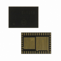
SI1011-A-GM Silicon Laboratories Inc, SI1011-A-GM Datasheet - Page 43

SI1011-A-GM
Manufacturer Part Number
SI1011-A-GM
Description
IC TXRX MCU + EZRADIOPRO
Manufacturer
Silicon Laboratories Inc
Specifications of SI1011-A-GM
Package / Case
42-QFN
Frequency
240MHz ~ 960MHz
Data Rate - Maximum
256kbps
Modulation Or Protocol
FSK, GFSK, OOK
Applications
General Purpose
Power - Output
20dBm
Sensitivity
-121dBm
Voltage - Supply
1.8 V ~ 3.6 V
Current - Receiving
18.5mA
Current - Transmitting
85mA
Data Interface
PCB, Surface Mount
Memory Size
8kB Flash, 768B RAM
Antenna Connector
PCB, Surface Mount
Number Of Receivers
1
Number Of Transmitters
1
Wireless Frequency
240 MHz to 960 MHz
Interface Type
UART, SMBus, SPI, PCA
Output Power
20 dBm
Operating Supply Voltage
0.9 V to 3.6 V
Maximum Operating Temperature
+ 85 C
Mounting Style
SMD/SMT
Maximum Supply Current
4 mA
Minimum Operating Temperature
- 40 C
Modulation
FSK, GFSK, OOK
Protocol Supported
C2, SMBus
Core
8051
Program Memory Type
Flash
Program Memory Size
8 KB
Data Ram Size
768 B
Supply Current (max)
4 mA
Lead Free Status / RoHS Status
Lead free / RoHS Compliant
Operating Temperature
-
Lead Free Status / Rohs Status
Lead free / RoHS Compliant
Other names
336-1872-5
Available stocks
Company
Part Number
Manufacturer
Quantity
Price
Company:
Part Number:
SI1011-A-GM
Manufacturer:
Silicon Laboratories Inc
Quantity:
135
- Current page: 43 of 384
- Download datasheet (3Mb)
General
PCB Design
Solder Mask Design
Stencil Design
Card Assembly
1.
2.
1.
2.
3.
1.
1.
2.
3.
4.
5.
1.
2.
All dimensions shown are in millimeters (mm) unless otherwise noted.
This land pattern design is based on the IPC-7351 guidelines.
High-Tg PCB materials (Glass Transition Temperature > 170° C are recommended for Pb-free reflow profiles per standard industry practice.
PCB design must ensure sufficient thermal relief for operation of the device.
Via placement must minimize mechanical stress due to CTE mismatch between PCB material and the package while maintaining electrical or
thermal performance as required for the particular application.
conductivity.
materials and total thermal relief provided by internal Cu plane in the PCB.
All metal pads are to be non-solder mask defined (NSMD). Clearance between the solder mask and the metal pad should be 60 µm minimum
around the pad.
A stainless steel, laser-cut and electro-polished stencil with trapezoidal walls should be used to assure good solder paste release.
The stencil thickness should be 0.125 mm (5 mils).
The ratio of stencil aperture to land pad size should be 1:1 for all perimeter pads.
A 3x3 array of 0.7 mm square openings on 0.9 mm pitch should be used for the upper center ground pad.
A 3x3 array of 0.8 mm square openings on 1.0 mm pitch should be used for the lower center ground pad.
A No-Clean, Type-3 solder paste is recommended.
The recommended card reflow profile is per the JEDEC/IPC J-STD-020 specification for Small Body Components.
a. A minimum of four vias are required under each E-pad; eight or more vias are recommended for designs that require increased thermal
b. Via diameters should be between 0.20 and 0.31 mm (8 to 12 mil).
c. Metal-to-metal distance between outer edge of via diameter and closest edge of device perimeter pad must be > 1.00 mm (dimension "K").
d. Vias may be placed as desired within the non-hatched area of the E-pads. Final via size and quantity is dependent on choice of PCB
e. Vias should either be filled or tented on the top-side of the board to prevent solder from migrating away from the E-pads during reflow.
Dimension
X1 (27x)
Y1 (27x)
X2 (15x)
Y2 (15x)
C1
C2
X3
X4
Y4
Y5
X6
Y6
X7
Y7
E
K
Table 3.3. PCB Land Pattern
Rev. 1.0
Si1010/1/2/3/4/5
Value
>1.00
0.125
4.75
0.95
0.30
7.00
0.30
0.70
0.50
2.73
2.63
1.59
3.16
2.97
0.07
1.42
43
Related parts for SI1011-A-GM
Image
Part Number
Description
Manufacturer
Datasheet
Request
R
Part Number:
Description:
QFN 42/I�/8KB, 768B RAM, +20 DBM, PROGRAMMABLE XCVR
Manufacturer:
Silicon Laboratories Inc
Part Number:
Description:
SMD/C�/SINGLE-ENDED OUTPUT SILICON OSCILLATOR
Manufacturer:
Silicon Laboratories Inc
Part Number:
Description:
Manufacturer:
Silicon Laboratories Inc
Datasheet:
Part Number:
Description:
N/A N/A/SI4010 AES KEYFOB DEMO WITH LCD RX
Manufacturer:
Silicon Laboratories Inc
Datasheet:
Part Number:
Description:
N/A N/A/SI4010 SIMPLIFIED KEY FOB DEMO WITH LED RX
Manufacturer:
Silicon Laboratories Inc
Datasheet:
Part Number:
Description:
N/A/-40 TO 85 OC/EZLINK MODULE; F930/4432 HIGH BAND (REV E/B1)
Manufacturer:
Silicon Laboratories Inc
Part Number:
Description:
EZLink Module; F930/4432 Low Band (rev e/B1)
Manufacturer:
Silicon Laboratories Inc
Part Number:
Description:
I�/4460 10 DBM RADIO TEST CARD 434 MHZ
Manufacturer:
Silicon Laboratories Inc
Part Number:
Description:
I�/4461 14 DBM RADIO TEST CARD 868 MHZ
Manufacturer:
Silicon Laboratories Inc
Part Number:
Description:
I�/4463 20 DBM RFSWITCH RADIO TEST CARD 460 MHZ
Manufacturer:
Silicon Laboratories Inc
Part Number:
Description:
I�/4463 20 DBM RADIO TEST CARD 868 MHZ
Manufacturer:
Silicon Laboratories Inc
Part Number:
Description:
I�/4463 27 DBM RADIO TEST CARD 868 MHZ
Manufacturer:
Silicon Laboratories Inc
Part Number:
Description:
I�/4463 SKYWORKS 30 DBM RADIO TEST CARD 915 MHZ
Manufacturer:
Silicon Laboratories Inc
Part Number:
Description:
N/A N/A/-40 TO 85 OC/4463 RFMD 30 DBM RADIO TEST CARD 915 MHZ
Manufacturer:
Silicon Laboratories Inc


