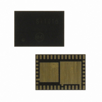
SI1011-A-GM Silicon Laboratories Inc, SI1011-A-GM Datasheet - Page 244

SI1011-A-GM
Manufacturer Part Number
SI1011-A-GM
Description
IC TXRX MCU + EZRADIOPRO
Manufacturer
Silicon Laboratories Inc
Specifications of SI1011-A-GM
Package / Case
42-QFN
Frequency
240MHz ~ 960MHz
Data Rate - Maximum
256kbps
Modulation Or Protocol
FSK, GFSK, OOK
Applications
General Purpose
Power - Output
20dBm
Sensitivity
-121dBm
Voltage - Supply
1.8 V ~ 3.6 V
Current - Receiving
18.5mA
Current - Transmitting
85mA
Data Interface
PCB, Surface Mount
Memory Size
8kB Flash, 768B RAM
Antenna Connector
PCB, Surface Mount
Number Of Receivers
1
Number Of Transmitters
1
Wireless Frequency
240 MHz to 960 MHz
Interface Type
UART, SMBus, SPI, PCA
Output Power
20 dBm
Operating Supply Voltage
0.9 V to 3.6 V
Maximum Operating Temperature
+ 85 C
Mounting Style
SMD/SMT
Maximum Supply Current
4 mA
Minimum Operating Temperature
- 40 C
Modulation
FSK, GFSK, OOK
Protocol Supported
C2, SMBus
Core
8051
Program Memory Type
Flash
Program Memory Size
8 KB
Data Ram Size
768 B
Supply Current (max)
4 mA
Lead Free Status / RoHS Status
Lead free / RoHS Compliant
Operating Temperature
-
Lead Free Status / Rohs Status
Lead free / RoHS Compliant
Other names
336-1872-5
Available stocks
Company
Part Number
Manufacturer
Quantity
Price
Company:
Part Number:
SI1011-A-GM
Manufacturer:
Silicon Laboratories Inc
Quantity:
135
- Current page: 244 of 384
- Download datasheet (3Mb)
Si1010/1/2/3/4/5
22.6. SPI Special Function Registers
SPI1 is accessed and controlled through four special function registers in the system controller: SPI1CN
Control Register, SPI1DAT Data Register, SPI1CFG Configuration Register, and SPI1CKR Clock Rate
Register. The special function registers related to the operation of the SPI1 Bus are described in the follow-
ing figures.
SFR Definition 22.1. SPI1CFG: SPI Configuration
SFR Page = 0x0; SFR Address = 0x84
244
*Note: In master mode, data on MISO is sampled one SYSCLK before the end of each data bit, to provide maximum
Name
Reset
Bit
3:0
Type
7
6
5
4
Bit
settling time for the slave device. See Table 22.2 for timing parameters.
Reserved
SPIBSY
MSTEN
CKPHA
CKPOL
SPIBSY
Name
R
7
0
MSTEN
SPI Busy.
This bit is set to logic 1 when a SPI transfer is in progress.
Master Mode Enable.
When set to 1, enables master mode. This bit must be set to 1 to communicate
with the EZRadioPRO peripheral.
SPI Clock Phase.
0: Data centered on first edge of SCK period.
1: Data centered on second edge of SCK period.
SPI Clock Polarity.
0: SCK line low in idle state.
1: SCK line high in idle state.
Read = 0000, Write = don’t care.
R/W
6
0
CKPHA
R/W
5
0
CKPOL
R/W
Rev. 1.0
4
0
Function
R
3
0
*
*
R
2
1
R
1
1
R
0
1
Related parts for SI1011-A-GM
Image
Part Number
Description
Manufacturer
Datasheet
Request
R
Part Number:
Description:
QFN 42/I�/8KB, 768B RAM, +20 DBM, PROGRAMMABLE XCVR
Manufacturer:
Silicon Laboratories Inc
Part Number:
Description:
SMD/C�/SINGLE-ENDED OUTPUT SILICON OSCILLATOR
Manufacturer:
Silicon Laboratories Inc
Part Number:
Description:
Manufacturer:
Silicon Laboratories Inc
Datasheet:
Part Number:
Description:
N/A N/A/SI4010 AES KEYFOB DEMO WITH LCD RX
Manufacturer:
Silicon Laboratories Inc
Datasheet:
Part Number:
Description:
N/A N/A/SI4010 SIMPLIFIED KEY FOB DEMO WITH LED RX
Manufacturer:
Silicon Laboratories Inc
Datasheet:
Part Number:
Description:
N/A/-40 TO 85 OC/EZLINK MODULE; F930/4432 HIGH BAND (REV E/B1)
Manufacturer:
Silicon Laboratories Inc
Part Number:
Description:
EZLink Module; F930/4432 Low Band (rev e/B1)
Manufacturer:
Silicon Laboratories Inc
Part Number:
Description:
I�/4460 10 DBM RADIO TEST CARD 434 MHZ
Manufacturer:
Silicon Laboratories Inc
Part Number:
Description:
I�/4461 14 DBM RADIO TEST CARD 868 MHZ
Manufacturer:
Silicon Laboratories Inc
Part Number:
Description:
I�/4463 20 DBM RFSWITCH RADIO TEST CARD 460 MHZ
Manufacturer:
Silicon Laboratories Inc
Part Number:
Description:
I�/4463 20 DBM RADIO TEST CARD 868 MHZ
Manufacturer:
Silicon Laboratories Inc
Part Number:
Description:
I�/4463 27 DBM RADIO TEST CARD 868 MHZ
Manufacturer:
Silicon Laboratories Inc
Part Number:
Description:
I�/4463 SKYWORKS 30 DBM RADIO TEST CARD 915 MHZ
Manufacturer:
Silicon Laboratories Inc
Part Number:
Description:
N/A N/A/-40 TO 85 OC/4463 RFMD 30 DBM RADIO TEST CARD 915 MHZ
Manufacturer:
Silicon Laboratories Inc


