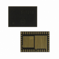
SI1011-A-GM Silicon Laboratories Inc, SI1011-A-GM Datasheet - Page 310

SI1011-A-GM
Manufacturer Part Number
SI1011-A-GM
Description
IC TXRX MCU + EZRADIOPRO
Manufacturer
Silicon Laboratories Inc
Specifications of SI1011-A-GM
Package / Case
42-QFN
Frequency
240MHz ~ 960MHz
Data Rate - Maximum
256kbps
Modulation Or Protocol
FSK, GFSK, OOK
Applications
General Purpose
Power - Output
20dBm
Sensitivity
-121dBm
Voltage - Supply
1.8 V ~ 3.6 V
Current - Receiving
18.5mA
Current - Transmitting
85mA
Data Interface
PCB, Surface Mount
Memory Size
8kB Flash, 768B RAM
Antenna Connector
PCB, Surface Mount
Number Of Receivers
1
Number Of Transmitters
1
Wireless Frequency
240 MHz to 960 MHz
Interface Type
UART, SMBus, SPI, PCA
Output Power
20 dBm
Operating Supply Voltage
0.9 V to 3.6 V
Maximum Operating Temperature
+ 85 C
Mounting Style
SMD/SMT
Maximum Supply Current
4 mA
Minimum Operating Temperature
- 40 C
Modulation
FSK, GFSK, OOK
Protocol Supported
C2, SMBus
Core
8051
Program Memory Type
Flash
Program Memory Size
8 KB
Data Ram Size
768 B
Supply Current (max)
4 mA
Lead Free Status / RoHS Status
Lead free / RoHS Compliant
Operating Temperature
-
Lead Free Status / Rohs Status
Lead free / RoHS Compliant
Other names
336-1872-5
Available stocks
Company
Part Number
Manufacturer
Quantity
Price
Company:
Part Number:
SI1011-A-GM
Manufacturer:
Silicon Laboratories Inc
Quantity:
135
- Current page: 310 of 384
- Download datasheet (3Mb)
Si1010/1/2/3/4/5
Figure 24.5 shows a typical master write sequence. Two transmit data bytes are shown, though any num-
ber of bytes may be transmitted. Notice that all of the ‘data byte transferred’ interrupts occur after the ACK
cycle in this mode, regardless of whether hardware ACK generation is enabled.
24.5.2. Read Sequence (Master)
During a read sequence, an SMBus master reads data from a slave device. The master in this transfer will
be a transmitter during the address byte, and a receiver during all data bytes. The SMBus interface gener-
ates the START condition and transmits the first byte containing the address of the target slave and the
data direction bit. In this case the data direction bit (R/W) will be logic 1 (READ). Serial data is then
received from the slave on SDA while the SMBus outputs the serial clock. The slave transmits one or more
bytes of serial data.
If hardware ACK generation is disabled, the ACKRQ is set to 1 and an interrupt is generated after each
received byte. Software must write the ACK bit at that time to ACK or NACK the received byte.
With hardware ACK generation enabled, the SMBus hardware will automatically generate the ACK/NACK,
and then post the interrupt. It is important to note that the appropriate ACK or NACK value should be
set up by the software prior to receiving the byte when hardware ACK generation is enabled.
Writing a 1 to the ACK bit generates an ACK; writing a 0 generates a NACK. Software should write a 0 to
the ACK bit for the last data transfer, to transmit a NACK. The interface exits Master Receiver Mode after
the STO bit is set and a STOP is generated. The interface will switch to Master Transmitter Mode if
SMB0DAT is written while an active Master Receiver. Figure 24.6 shows a typical master read sequence.
Two received data bytes are shown, though any number of bytes may be received. Notice that the “data
byte transferred” interrupts occur at different places in the sequence, depending on whether hardware ACK
generation is enabled. The interrupt occurs before the ACK with hardware ACK generation disabled, and
after the ACK when hardware ACK generation is enabled.
310
S
Received by SMBus
Interface
Transmitted by
SMBus Interface
SLA
Figure 24.5. Typical Master Write Sequence
Interrupts with Hardware ACK Disabled (EHACK = 0)
Interrupts with Hardware ACK Enabled (EHACK = 1)
W
A
Data Byte
Rev. 1.0
A
S = START
P = STOP
A = ACK
W = WRITE
SLA = Slave Address
Data Byte
A
P
Related parts for SI1011-A-GM
Image
Part Number
Description
Manufacturer
Datasheet
Request
R
Part Number:
Description:
QFN 42/I�/8KB, 768B RAM, +20 DBM, PROGRAMMABLE XCVR
Manufacturer:
Silicon Laboratories Inc
Part Number:
Description:
SMD/C�/SINGLE-ENDED OUTPUT SILICON OSCILLATOR
Manufacturer:
Silicon Laboratories Inc
Part Number:
Description:
Manufacturer:
Silicon Laboratories Inc
Datasheet:
Part Number:
Description:
N/A N/A/SI4010 AES KEYFOB DEMO WITH LCD RX
Manufacturer:
Silicon Laboratories Inc
Datasheet:
Part Number:
Description:
N/A N/A/SI4010 SIMPLIFIED KEY FOB DEMO WITH LED RX
Manufacturer:
Silicon Laboratories Inc
Datasheet:
Part Number:
Description:
N/A/-40 TO 85 OC/EZLINK MODULE; F930/4432 HIGH BAND (REV E/B1)
Manufacturer:
Silicon Laboratories Inc
Part Number:
Description:
EZLink Module; F930/4432 Low Band (rev e/B1)
Manufacturer:
Silicon Laboratories Inc
Part Number:
Description:
I�/4460 10 DBM RADIO TEST CARD 434 MHZ
Manufacturer:
Silicon Laboratories Inc
Part Number:
Description:
I�/4461 14 DBM RADIO TEST CARD 868 MHZ
Manufacturer:
Silicon Laboratories Inc
Part Number:
Description:
I�/4463 20 DBM RFSWITCH RADIO TEST CARD 460 MHZ
Manufacturer:
Silicon Laboratories Inc
Part Number:
Description:
I�/4463 20 DBM RADIO TEST CARD 868 MHZ
Manufacturer:
Silicon Laboratories Inc
Part Number:
Description:
I�/4463 27 DBM RADIO TEST CARD 868 MHZ
Manufacturer:
Silicon Laboratories Inc
Part Number:
Description:
I�/4463 SKYWORKS 30 DBM RADIO TEST CARD 915 MHZ
Manufacturer:
Silicon Laboratories Inc
Part Number:
Description:
N/A N/A/-40 TO 85 OC/4463 RFMD 30 DBM RADIO TEST CARD 915 MHZ
Manufacturer:
Silicon Laboratories Inc


