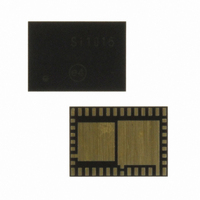
SI1011-A-GM Silicon Laboratories Inc, SI1011-A-GM Datasheet - Page 342

SI1011-A-GM
Manufacturer Part Number
SI1011-A-GM
Description
IC TXRX MCU + EZRADIOPRO
Manufacturer
Silicon Laboratories Inc
Specifications of SI1011-A-GM
Package / Case
42-QFN
Frequency
240MHz ~ 960MHz
Data Rate - Maximum
256kbps
Modulation Or Protocol
FSK, GFSK, OOK
Applications
General Purpose
Power - Output
20dBm
Sensitivity
-121dBm
Voltage - Supply
1.8 V ~ 3.6 V
Current - Receiving
18.5mA
Current - Transmitting
85mA
Data Interface
PCB, Surface Mount
Memory Size
8kB Flash, 768B RAM
Antenna Connector
PCB, Surface Mount
Number Of Receivers
1
Number Of Transmitters
1
Wireless Frequency
240 MHz to 960 MHz
Interface Type
UART, SMBus, SPI, PCA
Output Power
20 dBm
Operating Supply Voltage
0.9 V to 3.6 V
Maximum Operating Temperature
+ 85 C
Mounting Style
SMD/SMT
Maximum Supply Current
4 mA
Minimum Operating Temperature
- 40 C
Modulation
FSK, GFSK, OOK
Protocol Supported
C2, SMBus
Core
8051
Program Memory Type
Flash
Program Memory Size
8 KB
Data Ram Size
768 B
Supply Current (max)
4 mA
Lead Free Status / RoHS Status
Lead free / RoHS Compliant
Operating Temperature
-
Lead Free Status / Rohs Status
Lead free / RoHS Compliant
Other names
336-1872-5
Available stocks
Company
Part Number
Manufacturer
Quantity
Price
Company:
Part Number:
SI1011-A-GM
Manufacturer:
Silicon Laboratories Inc
Quantity:
135
- Current page: 342 of 384
- Download datasheet (3Mb)
Si1010/1/2/3/4/5
27.1.4. Mode 3: Two 8-Bit Counter/Timers (Timer 0 Only)
In Mode 3, Timer 0 is configured as two separate 8-bit counter/timers held in TL0 and TH0. The coun-
ter/timer in TL0 is controlled using the Timer 0 control/status bits in TCON and TMOD: TR0, C/T0, GATE0
and TF0. TL0 can use either the system clock or an external input signal as its timebase. The TH0 register
is restricted to a timer function sourced by the system clock or prescaled clock. TH0 is enabled using the
Timer 1 run control bit TR1. TH0 sets the Timer 1 overflow flag TF1 on overflow and thus controls the
Timer 1 interrupt.
Timer 1 is inactive in Mode 3. When Timer 0 is operating in Mode 3, Timer 1 can be operated in Modes 0,
1 or 2, but cannot be clocked by external signals nor set the TF1 flag and generate an interrupt. However,
the Timer 1 overflow can be used to generate baud rates for the SMBus and/or UART, and/or initiate ADC
conversions. While Timer 0 is operating in Mode 3, Timer 1 run control is handled through its mode set-
tings. To run Timer 1 while Timer 0 is in Mode 3, set the Timer 1 Mode as 0, 1, or 2. To disable Timer 1,
configure it for Mode 3.
342
INT0
T0
Crossbar
Pre-scaled Clock
SYSCLK
IN0PL
GATE0
Figure 27.2. T0 Mode 2 Block Diagram
XOR
0
1
TR0
M
H
T
3
M
T
3
L
CKCON
M
T
H
2
M
T
2
L
0
1
M
T
1
M
T
0
S
C
A
1
S
C
A
Rev. 1.0
0
G
A
E
T
1
C
T
1
/
M
T
1
1
TMOD
M
T
1
0
TCLK
G
A
T
E
0
C
T
0
/
M
T
0
1
M
T
0
0
(8 bits)
(8 bits)
TH0
TL0
N
P
1
L
I
N
1
S
L
2
I
IT01CF
N
1
S
L
1
I
N
S
1
L
0
I
N
0
P
L
I
Reload
N
0
S
L
2
I
N
S
0
L
1
I
N
S
0
L
0
I
TR1
TR0
TF1
TF0
IE1
IT1
IE0
IT0
Interrupt
Related parts for SI1011-A-GM
Image
Part Number
Description
Manufacturer
Datasheet
Request
R
Part Number:
Description:
QFN 42/I�/8KB, 768B RAM, +20 DBM, PROGRAMMABLE XCVR
Manufacturer:
Silicon Laboratories Inc
Part Number:
Description:
SMD/C�/SINGLE-ENDED OUTPUT SILICON OSCILLATOR
Manufacturer:
Silicon Laboratories Inc
Part Number:
Description:
Manufacturer:
Silicon Laboratories Inc
Datasheet:
Part Number:
Description:
N/A N/A/SI4010 AES KEYFOB DEMO WITH LCD RX
Manufacturer:
Silicon Laboratories Inc
Datasheet:
Part Number:
Description:
N/A N/A/SI4010 SIMPLIFIED KEY FOB DEMO WITH LED RX
Manufacturer:
Silicon Laboratories Inc
Datasheet:
Part Number:
Description:
N/A/-40 TO 85 OC/EZLINK MODULE; F930/4432 HIGH BAND (REV E/B1)
Manufacturer:
Silicon Laboratories Inc
Part Number:
Description:
EZLink Module; F930/4432 Low Band (rev e/B1)
Manufacturer:
Silicon Laboratories Inc
Part Number:
Description:
I�/4460 10 DBM RADIO TEST CARD 434 MHZ
Manufacturer:
Silicon Laboratories Inc
Part Number:
Description:
I�/4461 14 DBM RADIO TEST CARD 868 MHZ
Manufacturer:
Silicon Laboratories Inc
Part Number:
Description:
I�/4463 20 DBM RFSWITCH RADIO TEST CARD 460 MHZ
Manufacturer:
Silicon Laboratories Inc
Part Number:
Description:
I�/4463 20 DBM RADIO TEST CARD 868 MHZ
Manufacturer:
Silicon Laboratories Inc
Part Number:
Description:
I�/4463 27 DBM RADIO TEST CARD 868 MHZ
Manufacturer:
Silicon Laboratories Inc
Part Number:
Description:
I�/4463 SKYWORKS 30 DBM RADIO TEST CARD 915 MHZ
Manufacturer:
Silicon Laboratories Inc
Part Number:
Description:
N/A N/A/-40 TO 85 OC/4463 RFMD 30 DBM RADIO TEST CARD 915 MHZ
Manufacturer:
Silicon Laboratories Inc


