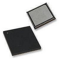
PIC18F65K90T-I/MR Microchip Technology, PIC18F65K90T-I/MR Datasheet - Page 191

PIC18F65K90T-I/MR
Manufacturer Part Number
PIC18F65K90T-I/MR
Description
32kB Flash, 2kB RAM, 1kB EE, NanoWatt XLP, LCD 64 QFN 9x9x0.9mm T/R
Manufacturer
Microchip Technology
Series
PIC® XLP™ 18Fr
Datasheet
1.PIC18F66K90-IMR.pdf
(570 pages)
Specifications of PIC18F65K90T-I/MR
Processor Series
PIC18F
Core
PIC
Data Bus Width
8 bit
Program Memory Type
Flash
Program Memory Size
32 KB
Data Ram Size
2 KB
Interface Type
I2C, SPI
Maximum Clock Frequency
64 MHz
Number Of Timers
8
Operating Supply Voltage
1.8 V to 5.5 V
Maximum Operating Temperature
+ 125 C
3rd Party Development Tools
52715-96, 52716-328, 52717-734, 52712-325, EWPIC18
Minimum Operating Temperature
- 40 C
On-chip Adc
12 bit, 16 Channel
Core Processor
PIC
Core Size
8-Bit
Speed
64MHz
Connectivity
I²C, LIN, SPI, UART/USART
Peripherals
Brown-out Detect/Reset, LCD, POR, PWM, WDT
Number Of I /o
53
Eeprom Size
1K x 8
Ram Size
2K x 8
Voltage - Supply (vcc/vdd)
1.8 V ~ 5.5 V
Data Converters
A/D 16x12b
Oscillator Type
Internal
Operating Temperature
-40°C ~ 85°C
Package / Case
64-VFQFN Exposed Pad
Lead Free Status / Rohs Status
Details
- Current page: 191 of 570
- Download datasheet (5Mb)
13.4
Timer1 can be configured for 16-bit reads and writes.
When the RD16 control bit (T1CON<1>) is set, the
address for TMR1H is mapped to a buffer register for
the high byte of Timer1. A read from TMR1L loads the
contents of the high byte of Timer1 into the Timer1 High
Byte Buffer register. This provides the user with the
ability to accurately read all 16 bits of Timer1 without
having to determine whether a read of the high byte,
followed by a read of the low byte, has become invalid
due to a rollover between reads.
A write to the high byte of Timer1 must also take place
through the TMR1H Buffer register. The Timer1 high
byte is updated with the contents of TMR1H when a
write occurs to TMR1L. This allows a user to write all
16 bits at once to both the high and low bytes of Timer1.
The high byte of Timer1 is not directly readable or
writable in this mode. All reads and writes must take
place through the Timer1 High Byte Buffer register.
Writes to TMR1H do not clear the Timer1 prescaler; the
prescaler is only cleared on writes to TMR1L.
13.5
An on-chip crystal oscillator circuit is incorporated
between pins, SOSCI (input) and SOSCO (amplifier
output). It is enabled by setting one of five bits: any of the
four SOSCEN bits in the TxCON registers (TxCON<3>)
or the SOSCGO bit in the OSCCON2 register
(OSCCON2<3>). The oscillator is a low-power circuit,
rated for 32 kHz crystals. It will continue to run during all
power-managed modes. The circuit for a typical LP
oscillator is depicted in
the capacitor selection for the SOSC oscillator.
The user must provide a software time delay to ensure
proper start-up of the SOSC oscillator.
FIGURE 13-2:
2009-2011 Microchip Technology Inc.
Note:
Timer1 16-Bit Read/Write Mode
SOSC Oscillator
12 pF
12 pF
C1
C2
See the Notes with
information about capacitor selection.
32.768 kHz
XTAL
Figure
EXTERNAL COMPONENTS
FOR THE SOSC
OSCILLATOR
13-2.
SOSCI
SOSCO
Table 13-2
PIC18F87K90
Table 13-2
for additional
provides
PIC18F87K90 FAMILY
TABLE 13-2:
The SOSC crystal oscillator drive level is determined
based on the SOSCSEL<1:0> (CONFIG1L<4:3>)
Configuration bits. The High Drive Level mode,
SOSCSEL<1:0> = 11, is intended to drive a wide
variety of 32.768 kHz crystals with a variety of load
capacitance (CL) ratings.
The Low Drive Level mode is highly optimized for
extremely low-power consumption. It is not intended to
drive all types of 32.768 kHz crystals. In the Low Drive
Level mode, the crystal oscillator circuit may not work
correctly if excessively large discrete capacitors are
placed on the SOSCO and SOSCI pins. This mode is
designed to work only with discrete capacitances of
approximately 3 pF-10 pF on each pin.
Crystal manufacturers usually specify a CL (Capaci-
tance Load) rating for their crystals. This value is
related to, but not necessarily the same as, the values
that should be used for C1 and C2 in
For more details on selecting the optimum C1 and C2
for a given crystal, see the crystal manufacture’s
applications information. The optimum value depends,
in part, on the amount of parasitic capacitance in the
circuit, which is often unknown. For that reason, it is
highly recommended that thorough testing and
validation of the oscillator be performed after values
have been selected.
Oscillator
Note 1: Microchip suggests these values as a
Type
LP
2: Higher capacitance increases the stabil-
3: Since each resonator/crystal has its own
4: Capacitor
5: Incorrect capacitance value may result in
starting point in validating the oscillator
circuit.
ity of the oscillator, but also increases the
start-up time.
characteristics, the user should consult
the resonator/crystal manufacturer for
appropriate
components.
guidance only. Values listed would be
typical of a CL = 10 pF rated crystal
when SOSCSEL<1:0> = 11.
a frequency not meeting the crystal
manufacturer’s tolerance specification.
32 kHz
Freq.
CAPACITOR SELECTION FOR
THE TIMER
OSCILLATOR
values
values
12 pF
C1
(2,3,4,5)
are
DS39957D-page 191
(1)
Figure
of
for
12 pF
13-2.
external
C2
design
(1)
Related parts for PIC18F65K90T-I/MR
Image
Part Number
Description
Manufacturer
Datasheet
Request
R

Part Number:
Description:
Manufacturer:
Microchip Technology Inc.
Datasheet:

Part Number:
Description:
Manufacturer:
Microchip Technology Inc.
Datasheet:

Part Number:
Description:
Manufacturer:
Microchip Technology Inc.
Datasheet:

Part Number:
Description:
Manufacturer:
Microchip Technology Inc.
Datasheet:

Part Number:
Description:
Manufacturer:
Microchip Technology Inc.
Datasheet:

Part Number:
Description:
Manufacturer:
Microchip Technology Inc.
Datasheet:

Part Number:
Description:
Manufacturer:
Microchip Technology Inc.
Datasheet:

Part Number:
Description:
Manufacturer:
Microchip Technology Inc.
Datasheet:


