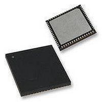
PIC18F65K90T-I/MR Microchip Technology, PIC18F65K90T-I/MR Datasheet - Page 278

PIC18F65K90T-I/MR
Manufacturer Part Number
PIC18F65K90T-I/MR
Description
32kB Flash, 2kB RAM, 1kB EE, NanoWatt XLP, LCD 64 QFN 9x9x0.9mm T/R
Manufacturer
Microchip Technology
Series
PIC® XLP™ 18Fr
Datasheet
1.PIC18F66K90-IMR.pdf
(570 pages)
Specifications of PIC18F65K90T-I/MR
Processor Series
PIC18F
Core
PIC
Data Bus Width
8 bit
Program Memory Type
Flash
Program Memory Size
32 KB
Data Ram Size
2 KB
Interface Type
I2C, SPI
Maximum Clock Frequency
64 MHz
Number Of Timers
8
Operating Supply Voltage
1.8 V to 5.5 V
Maximum Operating Temperature
+ 125 C
3rd Party Development Tools
52715-96, 52716-328, 52717-734, 52712-325, EWPIC18
Minimum Operating Temperature
- 40 C
On-chip Adc
12 bit, 16 Channel
Core Processor
PIC
Core Size
8-Bit
Speed
64MHz
Connectivity
I²C, LIN, SPI, UART/USART
Peripherals
Brown-out Detect/Reset, LCD, POR, PWM, WDT
Number Of I /o
53
Eeprom Size
1K x 8
Ram Size
2K x 8
Voltage - Supply (vcc/vdd)
1.8 V ~ 5.5 V
Data Converters
A/D 16x12b
Oscillator Type
Internal
Operating Temperature
-40°C ~ 85°C
Package / Case
64-VFQFN Exposed Pad
Lead Free Status / Rohs Status
Details
- Current page: 278 of 570
- Download datasheet (5Mb)
PIC18F87K90 FAMILY
The
functions of the port pins. Setting the segment enable
bit for a particular segment configures that pin as an
LCD driver. There are six LCD Segment Enable
registers, as shown in
LCDSEx register is shown in
TABLE 20-1:
REGISTER 20-5:
DS39957D-page 278
LCDSE0
LCDSE1
LCDSE2
LCDSE3
LCDSE4
LCDSE5
bit 7
Legend:
R = Readable bit
-n = Value at POR
bit 7-0
SE(n + 7)
R/W-0
Register
LCDSE5:LCDSE0
SE(n + 7):SE(n): Segment Enable bits
For LCDSE0: n = 0
For LCDSE1: n = 8
For LCDSE2: n = 16
For LCDSE3: n = 24
For LCDSE4: n = 32
For LCDSE5: n = 40
1 = Segment function of the pin is enabled, digital I/O is disabled
0 = I/O function of the pin is enabled
SE(n + 6)
LCDSE REGISTERS AND
ASSOCIATED SEGMENTS
R/W-0
39:32 (RJ<4:7>, RJ<3:1>, RC1)
LCDSEx: LCD SEGMENTx ENABLE REGISTER
47:40 (RH<0:3>, RH<7:4>)
15:8 (RA<5:4>, RC2, RC5,
RC<7:6>, RG4, RF<7:6>)
31:24 (RE7, RB0, RB5,
23:16 (RF<5:1>, RA1,
Table
registers
Register
7:0 (RD<7:0>)
W = Writable bit
‘1’ = Bit is set
SE(n + 5)
Segments
20-1. The prototype
RC<4:3>)
RB<4:1>)
R/W-0
20-5.
configure
SE(n + 4)
R/W-0
the
U = Unimplemented bit, read as ‘0’
‘0’ = Bit is cleared
SE(n + 3)
R/W-0
Once the module is initialized for the LCD panel, the
individual bits of the LCDDATA23:LCDDATA0 registers
are cleared or set to represent a clear or dark pixel,
respectively.
Specific sets of LCDDATA registers are used with
specific segments and common signals. Each bit
represents a unique combination of a specific segment
connected to a specific common.
Individual LCDDATA bits are named by the convention,
“SxxCy”, with “xx” as the segment number and “y” as
the common number. The relationship is summarized
in
shown in
Note:
Note:
Table
20-2. The prototype LCDDATAx register is
Register
The LCDSE5:LCDSE4 registers are not
implemented in PIC18F6XK90 devices.
In PIC18F6XK90 devices, writing into the
registers,
LCDDATA10, LCDDATA11, LCDDATA16,
LCDDATA17,
LCDDATA23, will not affect the status of
any pixel. These registers can be used as
general purpose registers.
SE(n + 2)
R/W-0
20-6.
2009-2011 Microchip Technology Inc.
LCDDATA4,
x = Bit is unknown
SE(n + 1)
R/W-0
LCDDATA22
LCDDATA5,
R/W-0
SE(n)
bit 0
and
Related parts for PIC18F65K90T-I/MR
Image
Part Number
Description
Manufacturer
Datasheet
Request
R

Part Number:
Description:
Manufacturer:
Microchip Technology Inc.
Datasheet:

Part Number:
Description:
Manufacturer:
Microchip Technology Inc.
Datasheet:

Part Number:
Description:
Manufacturer:
Microchip Technology Inc.
Datasheet:

Part Number:
Description:
Manufacturer:
Microchip Technology Inc.
Datasheet:

Part Number:
Description:
Manufacturer:
Microchip Technology Inc.
Datasheet:

Part Number:
Description:
Manufacturer:
Microchip Technology Inc.
Datasheet:

Part Number:
Description:
Manufacturer:
Microchip Technology Inc.
Datasheet:

Part Number:
Description:
Manufacturer:
Microchip Technology Inc.
Datasheet:


