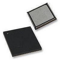
PIC18F65K90T-I/MR Microchip Technology, PIC18F65K90T-I/MR Datasheet - Page 505

PIC18F65K90T-I/MR
Manufacturer Part Number
PIC18F65K90T-I/MR
Description
32kB Flash, 2kB RAM, 1kB EE, NanoWatt XLP, LCD 64 QFN 9x9x0.9mm T/R
Manufacturer
Microchip Technology
Series
PIC® XLP™ 18Fr
Datasheet
1.PIC18F66K90-IMR.pdf
(570 pages)
Specifications of PIC18F65K90T-I/MR
Processor Series
PIC18F
Core
PIC
Data Bus Width
8 bit
Program Memory Type
Flash
Program Memory Size
32 KB
Data Ram Size
2 KB
Interface Type
I2C, SPI
Maximum Clock Frequency
64 MHz
Number Of Timers
8
Operating Supply Voltage
1.8 V to 5.5 V
Maximum Operating Temperature
+ 125 C
3rd Party Development Tools
52715-96, 52716-328, 52717-734, 52712-325, EWPIC18
Minimum Operating Temperature
- 40 C
On-chip Adc
12 bit, 16 Channel
Core Processor
PIC
Core Size
8-Bit
Speed
64MHz
Connectivity
I²C, LIN, SPI, UART/USART
Peripherals
Brown-out Detect/Reset, LCD, POR, PWM, WDT
Number Of I /o
53
Eeprom Size
1K x 8
Ram Size
2K x 8
Voltage - Supply (vcc/vdd)
1.8 V ~ 5.5 V
Data Converters
A/D 16x12b
Oscillator Type
Internal
Operating Temperature
-40°C ~ 85°C
Package / Case
64-VFQFN Exposed Pad
Lead Free Status / Rohs Status
Details
- Current page: 505 of 570
- Download datasheet (5Mb)
31.0
Absolute Maximum Ratings
Ambient temperature under bias.............................................................................................................-40°C to +125°C
Storage temperature .............................................................................................................................. -65°C to +150°C
Voltage on any digital only I/O pin with respect to V
Voltage on MCLR with respect to V
Voltage on any combined digital and analog pin with respect to V
Voltage on V
Voltage on V
Total power dissipation (Note 1) ..................................................................................................................................1W
Maximum current out of V
Maximum current into V
Input clamp current, I
Output clamp current, I
Maximum output current sunk by PORTA<7:6> and any PORTB and PORTC I/O pins.........................................25 mA
Maximum output current sunk by any PORTD, PORTE and PORTJ I/O pins ..........................................................8 mA
Maximum output current sunk by PORTA<5:0> and any PORTF, PORTG and PORTH I/O pins ............................2 mA
Maximum output current sourced by PORTA<7:6> and any PORTB and PORTC I/O pins ...................................25 mA
Maximum output current sourced by any PORTD, PORTE and PORTJ I/O pins .....................................................8 mA
Maximum output current sourced by PORTA<5:0> and any PORTF, PORTG and PORTH I/O pins .......................2 mA
Maximum current sunk by all ports combined.......................................................................................................200 mA
Note 1:
2009-2011 Microchip Technology Inc.
† NOTICE: Stresses above those listed under “Absolute Maximum Ratings” may cause permanent damage to the
device. This is a stress rating only and functional operation of the device at those or any other conditions above
those indicated in the operation listings of this specification is not implied. Exposure to maximum rating conditions
for extended periods may affect device reliability.
ELECTRICAL CHARACTERISTICS
Power dissipation is calculated as follows:
Pdis = V
DD
DD
with respect to V
with respect to V
DD
IK
x {I
OK
(V
DD
I
DD
SS
(V
< 0 or V
pin ..............................................................................................................................250 mA
O
pin ...........................................................................................................................300 mA
– I
< 0 or V
SS
SS
OH
I
SS
(regulator enabled) ............................................................................ -0.3V to 5.5V
(regulator disabled) ........................................................................... -0.3V to 3.6V
> V
(†)
} + {(V
........................................................................................................ -0.3V to +9.0V
O
DD
> V
) .......................................................................................................... ±20 mA
DD
DD
) ...................................................................................................±20 mA
– V
SS
OH
(except V
) x I
OH
PIC18F87K90 FAMILY
} + (V
DD
SS
)........................................................... -0.3V to 7.5V
(except V
OL
x I
OL
)
DD
and MCLR)...... -0.3V to (V
DS39957D-page 505
DD
+ 0.3V)
Related parts for PIC18F65K90T-I/MR
Image
Part Number
Description
Manufacturer
Datasheet
Request
R

Part Number:
Description:
Manufacturer:
Microchip Technology Inc.
Datasheet:

Part Number:
Description:
Manufacturer:
Microchip Technology Inc.
Datasheet:

Part Number:
Description:
Manufacturer:
Microchip Technology Inc.
Datasheet:

Part Number:
Description:
Manufacturer:
Microchip Technology Inc.
Datasheet:

Part Number:
Description:
Manufacturer:
Microchip Technology Inc.
Datasheet:

Part Number:
Description:
Manufacturer:
Microchip Technology Inc.
Datasheet:

Part Number:
Description:
Manufacturer:
Microchip Technology Inc.
Datasheet:

Part Number:
Description:
Manufacturer:
Microchip Technology Inc.
Datasheet:


