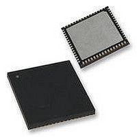
PIC18F65K90T-I/MR Microchip Technology, PIC18F65K90T-I/MR Datasheet - Page 303

PIC18F65K90T-I/MR
Manufacturer Part Number
PIC18F65K90T-I/MR
Description
32kB Flash, 2kB RAM, 1kB EE, NanoWatt XLP, LCD 64 QFN 9x9x0.9mm T/R
Manufacturer
Microchip Technology
Series
PIC® XLP™ 18Fr
Datasheet
1.PIC18F66K90-IMR.pdf
(570 pages)
Specifications of PIC18F65K90T-I/MR
Processor Series
PIC18F
Core
PIC
Data Bus Width
8 bit
Program Memory Type
Flash
Program Memory Size
32 KB
Data Ram Size
2 KB
Interface Type
I2C, SPI
Maximum Clock Frequency
64 MHz
Number Of Timers
8
Operating Supply Voltage
1.8 V to 5.5 V
Maximum Operating Temperature
+ 125 C
3rd Party Development Tools
52715-96, 52716-328, 52717-734, 52712-325, EWPIC18
Minimum Operating Temperature
- 40 C
On-chip Adc
12 bit, 16 Channel
Core Processor
PIC
Core Size
8-Bit
Speed
64MHz
Connectivity
I²C, LIN, SPI, UART/USART
Peripherals
Brown-out Detect/Reset, LCD, POR, PWM, WDT
Number Of I /o
53
Eeprom Size
1K x 8
Ram Size
2K x 8
Voltage - Supply (vcc/vdd)
1.8 V ~ 5.5 V
Data Converters
A/D 16x12b
Oscillator Type
Internal
Operating Temperature
-40°C ~ 85°C
Package / Case
64-VFQFN Exposed Pad
Lead Free Status / Rohs Status
Details
- Current page: 303 of 570
- Download datasheet (5Mb)
21.0
21.1
The Master Synchronous Serial Port (MSSP) module is
a serial interface, useful for communicating with other
peripheral or microcontroller devices. These peripheral
devices may be serial EEPROMs, shift registers,
display drivers, A/D Converters, etc. The MSSP
module can operate in one of two modes:
• Serial Peripheral Interface (SPI)
• Inter-Integrated Circuit (I
The I
hardware:
• Master mode
• Multi-Master mode
• Slave mode with 5-bit and 7-bit address masking
All members of the PIC18F87K90 family have two
MSSP modules, designated as MSSP1 and MSSP2.
Each module operates independently of the other.
21.2
Each MSSP module has three associated control regis-
ters. These include a status register (SSPxSTAT) and
two control registers (SSPxCON1 and SSPxCON2). The
use of these registers and their individual configuration
bits differ significantly depending on whether the MSSP
module is operated in SPI or I
Additional details are provided under the individual
sections.
2009-2011 Microchip Technology Inc.
- Full Master mode
- Slave mode (with general address call)
(with address masking for both 10-bit and 7-bit
addressing)
Note:
Note:
2
C interface supports the following modes in
MASTER SYNCHRONOUS
SERIAL PORT (MSSP)
MODULE
Master SSP (MSSP) Module
Overview
Control Registers
Throughout this section, generic refer-
ences to an MSSP module in any of its
operating modes may be interpreted as
being equally applicable to MSSP1 or
MSSP2. Register names and module I/O
signals use the generic designator ‘x’ to
indicate the use of a numeral to distinguish
a particular module when required. Control
bit names are not individuated.
In devices with more than one MSSP
module, it is very important to pay close
attention to SSPxCON register names.
SSP1CON1 and SSP1CON2 control
different operational aspects of the same
module,
SSP2CON1 control the same features for
two different modules.
while
2
C™)
2
C mode.
SSP1CON1
and
PIC18F87K90 FAMILY
21.3
The SPI mode allows 8 bits of data to be synchronously
transmitted and received simultaneously. All four
modes
communication, typically three pins are used:
• Serial Data Out (SDOx) – RC5/SDO1/SEG12 or
• Serial Data In (SDIx) – RC4/SDI1/SDA1/SEG16
• Serial Clock (SCKx) – RC3/SCK1/SCL1/SEG17
Additionally, a fourth pin may be used when in a Slave
mode of operation:
• Slave Select (SSx) – RF7/AN5/SS1/SEG25 or
Figure 21-1
module when operating in SPI mode.
FIGURE 21-1:
Note:
RD4/SEG4/SDO2
or RD5/SEG5/SDI2/SDA2
or RD6/SEG6/SCK2/SCL2
RD7/SEG7/SS2
SDOx
SCKx
SDIx
SSx
Only port I/O names are used in this diagram for
the sake of brevity. Refer to the text for a full list of
multiplexed functions.
SPI Mode
of
shows the block diagram of the MSSP
SPI
Read
SSx Control
are
Select
SMP:CKE
Edge
bit 0
Select
Edge
MSSPx BLOCK DIAGRAM
(SPI MODE)
Enable
SSPxBUF reg
Data to TXx/RXx in SSPxSR
TRIS bit
supported.
SSPxSR reg
2
Clock Select
SSPM<3:0>
4
2
DS39957D-page 303
(
Prescaler
4, 16, 64
TMR2 Output
To
Write
Clock
Shift
Data Bus
Internal
accomplish
2
T
OSC
)
Related parts for PIC18F65K90T-I/MR
Image
Part Number
Description
Manufacturer
Datasheet
Request
R

Part Number:
Description:
Manufacturer:
Microchip Technology Inc.
Datasheet:

Part Number:
Description:
Manufacturer:
Microchip Technology Inc.
Datasheet:

Part Number:
Description:
Manufacturer:
Microchip Technology Inc.
Datasheet:

Part Number:
Description:
Manufacturer:
Microchip Technology Inc.
Datasheet:

Part Number:
Description:
Manufacturer:
Microchip Technology Inc.
Datasheet:

Part Number:
Description:
Manufacturer:
Microchip Technology Inc.
Datasheet:

Part Number:
Description:
Manufacturer:
Microchip Technology Inc.
Datasheet:

Part Number:
Description:
Manufacturer:
Microchip Technology Inc.
Datasheet:


