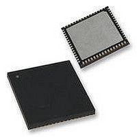
PIC18F65K90T-I/MR Microchip Technology, PIC18F65K90T-I/MR Datasheet - Page 538

PIC18F65K90T-I/MR
Manufacturer Part Number
PIC18F65K90T-I/MR
Description
32kB Flash, 2kB RAM, 1kB EE, NanoWatt XLP, LCD 64 QFN 9x9x0.9mm T/R
Manufacturer
Microchip Technology
Series
PIC® XLP™ 18Fr
Datasheet
1.PIC18F66K90-IMR.pdf
(570 pages)
Specifications of PIC18F65K90T-I/MR
Processor Series
PIC18F
Core
PIC
Data Bus Width
8 bit
Program Memory Type
Flash
Program Memory Size
32 KB
Data Ram Size
2 KB
Interface Type
I2C, SPI
Maximum Clock Frequency
64 MHz
Number Of Timers
8
Operating Supply Voltage
1.8 V to 5.5 V
Maximum Operating Temperature
+ 125 C
3rd Party Development Tools
52715-96, 52716-328, 52717-734, 52712-325, EWPIC18
Minimum Operating Temperature
- 40 C
On-chip Adc
12 bit, 16 Channel
Core Processor
PIC
Core Size
8-Bit
Speed
64MHz
Connectivity
I²C, LIN, SPI, UART/USART
Peripherals
Brown-out Detect/Reset, LCD, POR, PWM, WDT
Number Of I /o
53
Eeprom Size
1K x 8
Ram Size
2K x 8
Voltage - Supply (vcc/vdd)
1.8 V ~ 5.5 V
Data Converters
A/D 16x12b
Oscillator Type
Internal
Operating Temperature
-40°C ~ 85°C
Package / Case
64-VFQFN Exposed Pad
Lead Free Status / Rohs Status
Details
- Current page: 538 of 570
- Download datasheet (5Mb)
PIC18F87K90 FAMILY
FIGURE 31-16:
TABLE 31-19: I
DS39957D-page 538
100
101
102
103
90
91
106
107
92
109
110
D102
Note 1:
Param.
No.
2:
SCLx
SDAx
In
SDAx
Out
Note:
T
T
T
T
T
T
T
T
T
T
T
C
Symbol
SU
SU
SU
AA
HIGH
LOW
R
F
HD
HD
BUF
B
As a transmitter, the device must provide this internal minimum delay time to bridge the undefined region (min. 300 ns) of
the falling edge of SCLx to avoid unintended generation of Start or Stop conditions.
A Fast mode I
must then be met. This will automatically be the case if the device does not stretch the LOW period of the SCLx signal. If
such a device does stretch the LOW period of the SCLx signal, it must output the next data bit to the SDAx line,
T
is released.
R
:
:
:
:
:
STA
DAT
STO
STA
DAT
max. + T
Refer to
2
Clock High Time
Clock Low Time
SDAx and SCLx Rise Time 100 kHz mode
SDAx and SCLx Fall Time 100 kHz mode
Start Condition Setup Time 100 kHz mode
Start Condition Hold Time
Data Input Hold Time
Data Input Setup Time
Stop Condition Setup Time 100 kHz mode
Output Valid from Clock
Bus Free Time
Bus Capacitive Loading
C™ BUS DATA REQUIREMENTS (SLAVE MODE)
SU
I
2
90
2
:
C™ BUS DATA TIMING
Figure 31-3
DAT
C™ bus device can be used in a Standard mode I
103
= 1000 + 250 = 1250 ns (according to the Standard mode I
91
Characteristic
109
for load conditions.
100 kHz mode
400 kHz mode
MSSP module
100 kHz mode
400 kHz mode
MSSP module
400 kHz mode
400 kHz mode
400 kHz mode
100 kHz mode
400 kHz mode
100 kHz mode
400 kHz mode
100 kHz mode
400 kHz mode
400 kHz mode
100 kHz mode
400 kHz mode
100 kHz mode
400 kHz mode
100
106
101
109
20 + 0.1 C
20 + 0.1 C
107
1.5 T
1.5 T
Min
250
100
4.0
0.6
4.7
1.3
4.7
0.6
4.0
0.6
4.7
0.6
4.7
1.3
—
—
—
—
—
0
0
CY
CY
2
C bus system, but the requirement, T
B
B
1000
3500
Max
300
300
300
0.9
400
—
—
—
—
—
—
—
—
—
—
—
—
—
—
—
—
—
—
2
C bus specification), before the SCLx line
2009-2011 Microchip Technology Inc.
Units
pF
s
s
s
s
ns
ns
ns
ns
s
s
s
s
ns
s
ns
ns
s
s
ns
ns
s
s
C
10 to 400 pF
C
10 to 400 pF
Only relevant for Repeated
Start condition
After this period, the first clock
pulse is generated
(Note 2)
(Note 1)
Time the bus must be free before
a new transmission can start
92
B
B
102
is specified to be from
is specified to be from
110
Conditions
SU
:
DAT
250 ns,
Related parts for PIC18F65K90T-I/MR
Image
Part Number
Description
Manufacturer
Datasheet
Request
R

Part Number:
Description:
Manufacturer:
Microchip Technology Inc.
Datasheet:

Part Number:
Description:
Manufacturer:
Microchip Technology Inc.
Datasheet:

Part Number:
Description:
Manufacturer:
Microchip Technology Inc.
Datasheet:

Part Number:
Description:
Manufacturer:
Microchip Technology Inc.
Datasheet:

Part Number:
Description:
Manufacturer:
Microchip Technology Inc.
Datasheet:

Part Number:
Description:
Manufacturer:
Microchip Technology Inc.
Datasheet:

Part Number:
Description:
Manufacturer:
Microchip Technology Inc.
Datasheet:

Part Number:
Description:
Manufacturer:
Microchip Technology Inc.
Datasheet:


