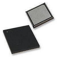
PIC18F65K90T-I/MR Microchip Technology, PIC18F65K90T-I/MR Datasheet - Page 421

PIC18F65K90T-I/MR
Manufacturer Part Number
PIC18F65K90T-I/MR
Description
32kB Flash, 2kB RAM, 1kB EE, NanoWatt XLP, LCD 64 QFN 9x9x0.9mm T/R
Manufacturer
Microchip Technology
Series
PIC® XLP™ 18Fr
Datasheet
1.PIC18F66K90-IMR.pdf
(570 pages)
Specifications of PIC18F65K90T-I/MR
Processor Series
PIC18F
Core
PIC
Data Bus Width
8 bit
Program Memory Type
Flash
Program Memory Size
32 KB
Data Ram Size
2 KB
Interface Type
I2C, SPI
Maximum Clock Frequency
64 MHz
Number Of Timers
8
Operating Supply Voltage
1.8 V to 5.5 V
Maximum Operating Temperature
+ 125 C
3rd Party Development Tools
52715-96, 52716-328, 52717-734, 52712-325, EWPIC18
Minimum Operating Temperature
- 40 C
On-chip Adc
12 bit, 16 Channel
Core Processor
PIC
Core Size
8-Bit
Speed
64MHz
Connectivity
I²C, LIN, SPI, UART/USART
Peripherals
Brown-out Detect/Reset, LCD, POR, PWM, WDT
Number Of I /o
53
Eeprom Size
1K x 8
Ram Size
2K x 8
Voltage - Supply (vcc/vdd)
1.8 V ~ 5.5 V
Data Converters
A/D 16x12b
Oscillator Type
Internal
Operating Temperature
-40°C ~ 85°C
Package / Case
64-VFQFN Exposed Pad
Lead Free Status / Rohs Status
Details
- Current page: 421 of 570
- Download datasheet (5Mb)
27.7
A unique feature on board the CTMU module is its ability
to generate system clock independent output pulses,
based on either an internal voltage or an external capac-
itor value. When using an external voltage, this is
accomplished using the CTDIN input pin as a trigger for
the pulse delay. When using an internal capacitor
value, this is accomplished using the internal compara-
tor voltage reference module and Comparator 2 input
pin. The pulse is output onto the CTPLS pin. To enable
this mode, set the TGEN bit.
See
CTMUDS (ODCON3<0>) is cleared, the pulse delay is
determined by the output of Comparator 2, and when it
is set, the pulse delay is determined by the input of
CTDIN. C
output pulse width on CTPLS. The pulse width is calcu-
lated by T = (C
current source measurement step (
“Current Source Calibration”
reference voltage (CV
FIGURE 27-4:
2009-2011 Microchip Technology Inc.
Figure 27-4
Creating a Delay with the CTMU
Module
DELAY
DELAY
is chosen by the user to determine the
for an example circuit. When
/I) * V, where I is known from the
REF
TYPICAL CONNECTIONS AND INTERNAL CONFIGURATION FOR PULSE
DELAY GENERATION
).
C
CTED1
CTMUI
DELAY
) and V is the internal
Section 27.4.1
External Reference
EDG1
CV
External Comparator
Current Source
REF
PIC18F87K90
Comparator
CTMU
C2
PIC18F87K90 FAMILY
An example use of the external capacitor feature is
interfacing with variable capacitive-based sensors,
such as a humidity sensor. As the humidity varies, the
pulse-width output on CTPLS will vary. An example use
of the CTDIN feature is interfacing with a digital sensor.
The CTPLS output pin can be connected to an input
capture pin and the varying pulse width measured to
determine the humidity in the application.
To use this feature:
1.
2.
3.
4.
When CTMUDS is cleared, as soon as C
to the value of the voltage reference trip point, an output
pulse is generated on CTPLS. When CTMUDS is set, as
soon as CTDIN is set, an output pulse is generated on
CTPLS.
C1
If CTMUDS is cleared, initialize Comparator 2.
If CTMUDS is cleared, initialize the comparator
voltage reference.
Initialize the CTMU and enable time delay
generation by setting the TGEN bit.
Set EDG1STAT.
CTDIN
CTPLS
CTMUDS
DS39957D-page 421
DELAY
charges
Related parts for PIC18F65K90T-I/MR
Image
Part Number
Description
Manufacturer
Datasheet
Request
R

Part Number:
Description:
Manufacturer:
Microchip Technology Inc.
Datasheet:

Part Number:
Description:
Manufacturer:
Microchip Technology Inc.
Datasheet:

Part Number:
Description:
Manufacturer:
Microchip Technology Inc.
Datasheet:

Part Number:
Description:
Manufacturer:
Microchip Technology Inc.
Datasheet:

Part Number:
Description:
Manufacturer:
Microchip Technology Inc.
Datasheet:

Part Number:
Description:
Manufacturer:
Microchip Technology Inc.
Datasheet:

Part Number:
Description:
Manufacturer:
Microchip Technology Inc.
Datasheet:

Part Number:
Description:
Manufacturer:
Microchip Technology Inc.
Datasheet:


