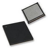
PIC18F65K90T-I/MR Microchip Technology, PIC18F65K90T-I/MR Datasheet - Page 192

PIC18F65K90T-I/MR
Manufacturer Part Number
PIC18F65K90T-I/MR
Description
32kB Flash, 2kB RAM, 1kB EE, NanoWatt XLP, LCD 64 QFN 9x9x0.9mm T/R
Manufacturer
Microchip Technology
Series
PIC® XLP™ 18Fr
Datasheet
1.PIC18F66K90-IMR.pdf
(570 pages)
Specifications of PIC18F65K90T-I/MR
Processor Series
PIC18F
Core
PIC
Data Bus Width
8 bit
Program Memory Type
Flash
Program Memory Size
32 KB
Data Ram Size
2 KB
Interface Type
I2C, SPI
Maximum Clock Frequency
64 MHz
Number Of Timers
8
Operating Supply Voltage
1.8 V to 5.5 V
Maximum Operating Temperature
+ 125 C
3rd Party Development Tools
52715-96, 52716-328, 52717-734, 52712-325, EWPIC18
Minimum Operating Temperature
- 40 C
On-chip Adc
12 bit, 16 Channel
Core Processor
PIC
Core Size
8-Bit
Speed
64MHz
Connectivity
I²C, LIN, SPI, UART/USART
Peripherals
Brown-out Detect/Reset, LCD, POR, PWM, WDT
Number Of I /o
53
Eeprom Size
1K x 8
Ram Size
2K x 8
Voltage - Supply (vcc/vdd)
1.8 V ~ 5.5 V
Data Converters
A/D 16x12b
Oscillator Type
Internal
Operating Temperature
-40°C ~ 85°C
Package / Case
64-VFQFN Exposed Pad
Lead Free Status / Rohs Status
Details
- Current page: 192 of 570
- Download datasheet (5Mb)
PIC18F87K90 FAMILY
13.5.1
The SOSC oscillator is also available as a clock source
in power-managed modes. By setting the System
Clock Select bits, SCS<1:0> (OSCCON<1:0>), to ‘01’,
the device switches to SEC_RUN mode, and both the
CPU and peripherals are clocked from the SOSC oscil-
lator. If the IDLEN bit (OSCCON<7>) is cleared and a
SLEEP instruction is executed, the device enters
SEC_IDLE mode. Additional details are available in
Section 4.0 “Power-Managed
Whenever the SOSC oscillator is providing the clock
source, the SOSC System Clock Status Flag, SOSC-
RUN (OSCCON2<6>), is set. This can be used to
determine the controller’s current clocking mode. It can
also indicate the clock source currently being used by
the Fail-Safe Clock Monitor (FSCM).
If the Clock Monitor is enabled and the SOSC oscillator
fails while providing the clock, polling the SOCSRUN
bit will indicate whether the clock is being provided by
the SOSC oscillator or another source.
13.5.2
The SOSC oscillator circuit draws very little power
during operation. Due to the low-power nature of the
oscillator, it may also be sensitive to rapidly changing
signals in close proximity. This is especially true when
the oscillator is configured for extremely low-power
mode (CONFIG1L<4:3> (SOSCSEL) = 01).
The oscillator circuit, displayed in
be located as close as possible to the microcontroller.
There should be no circuits passing within the oscillator
circuit boundaries other than V
If a high-speed circuit must be located near the oscillator,
it may help to have a grounded guard ring around the
oscillator circuit. The guard, as displayed in
could be used on a single-sided PCB or in addition to a
ground plane. (Examples of a high-speed circuit include
the ECCP1 pin, in Output Compare or PWM mode, or
the primary oscillator using the OSC2 pin.)
DS39957D-page 192
USING SOSC AS A
CLOCK SOURCE
SOSC OSCILLATOR LAYOUT
CONSIDERATIONS
SS
Modes”.
or V
Figure
DD
.
13-2, should
Figure
13-3,
FIGURE 13-3:
In the Low Drive Level mode, SOSCSEL<1:0> = 01, it
is critical that RC2 I/O pin signals be kept away from the
oscillator circuit. Configuring RC2 as a digital output,
and toggling it, can potentially disturb the oscillator cir-
cuit, even with a relatively good PCB layout. If possible,
either leave RC2 unused or use it as an input pin with
a slew rate limited signal source. If RC2 must be used
as a digital output, it may be necessary to use the High
Drive Level Oscillator mode (SOSCSEL<1:0> = 11)
with many PCB layouts.
Even in the High Drive Level mode, careful layout
procedures should still be followed when designing the
oscillator circuit.
In addition to dV/dt induced noise considerations, it is
important to ensure that the circuit board is clean. Even
a very small amount of conductive soldering flux
residue can cause PCB leakage currents that can
overwhelm the oscillator circuit.
13.6
The TMR1 register pair (TMR1H:TMR1L) increments
from 0000h to FFFFh and rolls over to 0000h. The
Timer1 interrupt, if enabled, is generated on overflow
which is latched in the Timer1 Overflow Interrupt Flag
bit, TMR1IF (PIR1<0>). This interrupt can be enabled
or disabled by setting or clearing the Timer1 Interrupt
Enable bit, TMR1IE (PIE1<0>).
Note: Not drawn to scale.
Timer1 Interrupt
2009-2011 Microchip Technology Inc.
OSCILLATOR CIRCUIT
WITH GROUNDED
GUARD RING
V
V
OSC1
OSC2
RC0
RC1
RC2
DD
SS
Related parts for PIC18F65K90T-I/MR
Image
Part Number
Description
Manufacturer
Datasheet
Request
R

Part Number:
Description:
Manufacturer:
Microchip Technology Inc.
Datasheet:

Part Number:
Description:
Manufacturer:
Microchip Technology Inc.
Datasheet:

Part Number:
Description:
Manufacturer:
Microchip Technology Inc.
Datasheet:

Part Number:
Description:
Manufacturer:
Microchip Technology Inc.
Datasheet:

Part Number:
Description:
Manufacturer:
Microchip Technology Inc.
Datasheet:

Part Number:
Description:
Manufacturer:
Microchip Technology Inc.
Datasheet:

Part Number:
Description:
Manufacturer:
Microchip Technology Inc.
Datasheet:

Part Number:
Description:
Manufacturer:
Microchip Technology Inc.
Datasheet:


