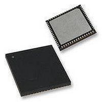
PIC18F65K90T-I/MR Microchip Technology, PIC18F65K90T-I/MR Datasheet - Page 335

PIC18F65K90T-I/MR
Manufacturer Part Number
PIC18F65K90T-I/MR
Description
32kB Flash, 2kB RAM, 1kB EE, NanoWatt XLP, LCD 64 QFN 9x9x0.9mm T/R
Manufacturer
Microchip Technology
Series
PIC® XLP™ 18Fr
Datasheet
1.PIC18F66K90-IMR.pdf
(570 pages)
Specifications of PIC18F65K90T-I/MR
Processor Series
PIC18F
Core
PIC
Data Bus Width
8 bit
Program Memory Type
Flash
Program Memory Size
32 KB
Data Ram Size
2 KB
Interface Type
I2C, SPI
Maximum Clock Frequency
64 MHz
Number Of Timers
8
Operating Supply Voltage
1.8 V to 5.5 V
Maximum Operating Temperature
+ 125 C
3rd Party Development Tools
52715-96, 52716-328, 52717-734, 52712-325, EWPIC18
Minimum Operating Temperature
- 40 C
On-chip Adc
12 bit, 16 Channel
Core Processor
PIC
Core Size
8-Bit
Speed
64MHz
Connectivity
I²C, LIN, SPI, UART/USART
Peripherals
Brown-out Detect/Reset, LCD, POR, PWM, WDT
Number Of I /o
53
Eeprom Size
1K x 8
Ram Size
2K x 8
Voltage - Supply (vcc/vdd)
1.8 V ~ 5.5 V
Data Converters
A/D 16x12b
Oscillator Type
Internal
Operating Temperature
-40°C ~ 85°C
Package / Case
64-VFQFN Exposed Pad
Lead Free Status / Rohs Status
Details
- Current page: 335 of 570
- Download datasheet (5Mb)
21.4.7
In I
reload value is placed in the lower 7 bits of the
SSPxADD register
occurs to SSPxBUF, the Baud Rate Generator will
automatically begin counting. The BRG counts down to
0 and stops until another reload has taken place. The
BRG count is decremented twice per instruction cycle
(T
BRG is reloaded automatically.
Once the given operation is complete (i.e., transmis-
sion of the last data bit is followed by ACK), the internal
clock will automatically stop counting and the SCLx pin
will remain in its last state.
Table 21-3
instruction cycles and the BRG value loaded into
SSPxADD. The SSPxADD BRG value of ‘0x00’ is not
supported.
FIGURE 21-19:
TABLE 21-3:
2009-2011 Microchip Technology Inc.
Note 1:
CY
2
C Master mode, the Baud Rate Generator (BRG)
) on the Q2 and Q4 clocks. In I
16 MHz
40 MHz
40 MHz
40 MHz
16 MHz
16 MHz
16 MHz
4 MHz
4 MHz
F
OSC
A minimum of 16 MHz F
BAUD RATE
demonstrates clock rates based on
(1)
I
2
C™ CLOCK RATE w/BRG
(Figure
BAUD RATE GENERATOR BLOCK DIAGRAM
SSPM<3:0>
21-19). When a write
SCLx
10 MHz
10 MHz
10 MHz
4 MHz
4 MHz
4 MHz
1 MHz
1 MHz
4 MHz
F
2
CY
C Master mode, the
OSC
is required to get the 1 MHz I
SSPM<3:0>
Control
Reload
CLKO
20 MHz
20 MHz
20 MHz
F
8 MHz
8 MHz
8 MHz
2 MHz
2 MHz
8 MHz
CY
Reload
* 2
PIC18F87K90 FAMILY
BRG Down Counter
21.4.7.1
Because MSSP1 and MSSP2 are independent, they
can operate simultaneously in I
different baud rates. This is done by using different
BRG reload values for each module.
Because this mode derives its basic clock source from
the system clock, any changes to the clock will affect
both modules in the same proportion. It may be
possible to change one or both baud rates back to a
previous value by changing the BRG reload value.
SSPxADD<6:0>
2
C.
BRG Value
Baud Rate and Module
Interdependence
0Ch
18h
1Fh
63h
09h
27h
02h
09h
03h
F
OSC
/4
(2 Rollovers of BRG)
2
C Master mode at
DS39957D-page 335
312.5 kHz
1 MHz
400 kHz
100 kHz
400 kHz
308 kHz
100 kHz
333 kHz
100 kHz
F
SCL
(1)
Related parts for PIC18F65K90T-I/MR
Image
Part Number
Description
Manufacturer
Datasheet
Request
R

Part Number:
Description:
Manufacturer:
Microchip Technology Inc.
Datasheet:

Part Number:
Description:
Manufacturer:
Microchip Technology Inc.
Datasheet:

Part Number:
Description:
Manufacturer:
Microchip Technology Inc.
Datasheet:

Part Number:
Description:
Manufacturer:
Microchip Technology Inc.
Datasheet:

Part Number:
Description:
Manufacturer:
Microchip Technology Inc.
Datasheet:

Part Number:
Description:
Manufacturer:
Microchip Technology Inc.
Datasheet:

Part Number:
Description:
Manufacturer:
Microchip Technology Inc.
Datasheet:

Part Number:
Description:
Manufacturer:
Microchip Technology Inc.
Datasheet:


