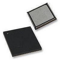
PIC18F65K90T-I/MR Microchip Technology, PIC18F65K90T-I/MR Datasheet - Page 242

PIC18F65K90T-I/MR
Manufacturer Part Number
PIC18F65K90T-I/MR
Description
32kB Flash, 2kB RAM, 1kB EE, NanoWatt XLP, LCD 64 QFN 9x9x0.9mm T/R
Manufacturer
Microchip Technology
Series
PIC® XLP™ 18Fr
Datasheet
1.PIC18F66K90-IMR.pdf
(570 pages)
Specifications of PIC18F65K90T-I/MR
Processor Series
PIC18F
Core
PIC
Data Bus Width
8 bit
Program Memory Type
Flash
Program Memory Size
32 KB
Data Ram Size
2 KB
Interface Type
I2C, SPI
Maximum Clock Frequency
64 MHz
Number Of Timers
8
Operating Supply Voltage
1.8 V to 5.5 V
Maximum Operating Temperature
+ 125 C
3rd Party Development Tools
52715-96, 52716-328, 52717-734, 52712-325, EWPIC18
Minimum Operating Temperature
- 40 C
On-chip Adc
12 bit, 16 Channel
Core Processor
PIC
Core Size
8-Bit
Speed
64MHz
Connectivity
I²C, LIN, SPI, UART/USART
Peripherals
Brown-out Detect/Reset, LCD, POR, PWM, WDT
Number Of I /o
53
Eeprom Size
1K x 8
Ram Size
2K x 8
Voltage - Supply (vcc/vdd)
1.8 V ~ 5.5 V
Data Converters
A/D 16x12b
Oscillator Type
Internal
Operating Temperature
-40°C ~ 85°C
Package / Case
64-VFQFN Exposed Pad
Lead Free Status / Rohs Status
Details
- Current page: 242 of 570
- Download datasheet (5Mb)
PIC18F87K90 FAMILY
18.1.2
When operating in Output mode (the Compare or PWM
modes), the drivers for the CCPx pins can be optionally
configured as open-drain outputs. This feature allows
the voltage level on the pin to be pulled to a higher level
through an external pull-up resistor and allows the
output to communicate with external circuits without the
need for additional level shifters.
The open-drain output option is controlled by the
CCPxOD bits (ODCON2<7:2>). Setting the appropriate
bit configures the pin for the corresponding module for
open-drain operation.
18.1.3
The pin assignment for CCP6/7/8/9 (Capture input,
Compare and PWM output) can change, based on the
device configuration.
The ECCPMX Configuration bit (CONFIG3H<1>)
determines the pin to which CCP6/7/8/9 is multiplexed.
The pin assignments for these CCP modules are given
in
TABLE 18-4:
DS39957D-page 242
ECCPMX
(Default)
Table
Value
1
0
18-4.
OPEN-DRAIN OUTPUT OPTION
PIN ASSIGNMENT FOR CCP6,
CCP7, CCP8 AND CCP9
CCP6
RH7
RE6
CCP PIN ASSIGNMENT
CCP7
Pin Mapped To
RH6
RE5
CCP8
RH5
RE4
CC9
RH4
RE3
18.2
In Capture mode, the CCPR4H:CCPR4L register pair
captures the 16-bit value of the TMR1 or TMR3 register
when an event occurs on the CCP4 pins. An event is
defined as one of the following:
• Every falling edge
• Every rising edge
• Every 4th rising edge
• Every 16th rising edge
The event is selected by the mode select bits,
CCP4M<3:0> (CCP4CON<3:0>). When a capture is
made, the interrupt request flag bit, CCP4IF (PIR4<1>),
is set. (It must be cleared in software.) If another
capture occurs before the value in CCPR4 is read, the
old captured value is overwritten by the new captured
value.
Figure 18-1
18.2.1
In Capture mode, the appropriate CCPx pin should be
configured as an input by setting the corresponding
TRIS direction bit.
18.2.2
For the available timers (1/3/5/7) to be used for the cap-
ture feature, the used timers must be running in Timer
mode or Synchronized Counter mode. In Asynchronous
Counter mode, the capture operation may not work.
The timer to be used with each CCP module is selected
in the CCPTMRSx registers. (See
Modules and Timer
Details of the timer assignments for the CCP modules
are given in
Note:
Capture Mode
shows the Capture mode block diagram.
CCP PIN CONFIGURATION
If RC1 or RE7 is configured as a CCP4
output, a write to the PORT causes a
capture condition.
TIMER1/3/5/7 MODE SELECTION
Table 18-2
2009-2011 Microchip Technology Inc.
Resources”.)
and
Table
18-3.
Section 18.1.1 “CCP
Related parts for PIC18F65K90T-I/MR
Image
Part Number
Description
Manufacturer
Datasheet
Request
R

Part Number:
Description:
Manufacturer:
Microchip Technology Inc.
Datasheet:

Part Number:
Description:
Manufacturer:
Microchip Technology Inc.
Datasheet:

Part Number:
Description:
Manufacturer:
Microchip Technology Inc.
Datasheet:

Part Number:
Description:
Manufacturer:
Microchip Technology Inc.
Datasheet:

Part Number:
Description:
Manufacturer:
Microchip Technology Inc.
Datasheet:

Part Number:
Description:
Manufacturer:
Microchip Technology Inc.
Datasheet:

Part Number:
Description:
Manufacturer:
Microchip Technology Inc.
Datasheet:

Part Number:
Description:
Manufacturer:
Microchip Technology Inc.
Datasheet:


