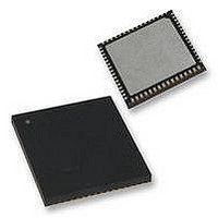
PIC18F65K90-I/MR Microchip Technology, PIC18F65K90-I/MR Datasheet - Page 153

PIC18F65K90-I/MR
Manufacturer Part Number
PIC18F65K90-I/MR
Description
32kB Flash, 2kB RAM, 1kB EE, NanoWatt XLP, LCD 64 QFN 9x9x0.9mm TUBE
Manufacturer
Microchip Technology
Series
PIC® XLP™ 18Fr
Datasheet
1.PIC18F65K90-IMR.pdf
(570 pages)
Specifications of PIC18F65K90-I/MR
Processor Series
PIC18F
Core
PIC
Data Bus Width
8 bit
Program Memory Type
Flash
Program Memory Size
32 KB
Data Ram Size
2 KB
Interface Type
I2C, SPI
Maximum Clock Frequency
64 MHz
Number Of Timers
8
Operating Supply Voltage
1.8 V to 5.5 V
Maximum Operating Temperature
+ 125 C
3rd Party Development Tools
52715-96, 52716-328, 52717-734, 52712-325, EWPIC18
Minimum Operating Temperature
- 40 C
On-chip Adc
12 bit, 16 Channel
Core Processor
PIC
Core Size
8-Bit
Speed
64MHz
Connectivity
I²C, LIN, SPI, UART/USART
Peripherals
Brown-out Detect/Reset, LCD, POR, PWM, WDT
Number Of I /o
53
Eeprom Size
1K x 8
Ram Size
2K x 8
Voltage - Supply (vcc/vdd)
1.8 V ~ 5.5 V
Data Converters
A/D 16x12b
Oscillator Type
Internal
Operating Temperature
-40°C ~ 85°C
Package / Case
64-VFQFN Exposed Pad
Lead Free Status / Rohs Status
Details
- Current page: 153 of 570
- Download datasheet (5Mb)
11.0
Depending on the device selected and features
enabled, there are up to nine ports available. Some
pins of the I/O ports are multiplexed with an alternate
function from the peripheral features on the device. In
general, when a peripheral is enabled, that pin may not
be used as a general purpose I/O pin.
Each port has three memory mapped registers for its
operation:
• TRIS register (Data Direction register)
• PORT register (reads the levels on the pins of the
• LAT register (Output Latch register)
Reading the PORT register reads the current status of
the pins, whereas writing to the PORT register writes to
the Output Latch (LAT) register.
Setting a TRIS bit (= 1) makes the corresponding port
pin an input (putting the corresponding output driver in
a High-Impedance mode). Clearing a TRIS bit (= 0)
makes the corresponding port pin an output (i.e., puts
the contents of the corresponding LAT bit on the
selected pin).
The Output Latch (LAT register) is useful for
read-modify-write operations on the value that the I/O
pins are driving. Read-modify-write operations on the
LAT register, read and write the latched output value for
the PORT register.
A simplified model of a generic I/O port, without the
interfaces to other peripherals, is shown in
FIGURE 11-1:
2009-2011 Microchip Technology Inc.
device)
Note:
RD LAT
Data
Bus
WR LAT
or PORT
WR TRIS
RD TRIS
RD PORT
I/O PORTS
I/O pins have diode protection to V
TRIS Latch
Data Latch
CKx
CKx
D
D
GENERIC I/O PORT
OPERATION
Q
Q
Q
EN
EN
D
DD
and V
Figure
Buffer
I/O Pin
Input
SS
.
11-1.
PIC18F87K90 FAMILY
11.1
When developing an application, the capabilities of the
port pins must be considered. Outputs on some pins
have higher output drive strength than others. Similarly,
some pins can tolerate higher than V
All of the digital ports are 5.5V input tolerant. The ana-
log ports have the same tolerance, having clamping
diodes implemented internally.
11.1.1
When used as digital I/O, the output pin drive strengths
vary, according to the pins’ grouping, to meet the needs
for a variety of applications. In general, there are two
classes of output pins, in terms of drive capability:
• Outputs designed to drive higher current loads,
• Outputs with lower drive levels, but capable of
For more details, see “Absolute Maximum Ratings” in
Section 31.0 “Electrical
Regardless of its port, all output pins in LCD Segment
or common-mode have sufficient output to directly
drive a display.
11.1.2
Four of the I/O ports (PORTB, PORTD, PORTE and
PORTJ) implement configurable weak pull-ups on all
pins. These are internal pull-ups that allow floating
digital input signals to be pulled to a consistent level
without the use of external resistors.
The pull-ups are enabled with a single bit for each of the
ports: RBPU (INTCON2<7>) for PORTB, and RDPU,
REPU and RJPU (PADCFG1<7:5>) for the other ports.
By setting RDPU, REPU and RJPU, each of the
pull-ups on these ports can be enabled. The pull-ups
are disabled on a POR event.
such as LEDs:
- PORTA
- PORTC
driving normal digital circuit loads with a high input
impedance. Also, able to drive LEDs, but only
those with smaller current requirements:
- PORTD
- PORTF
- PORTH
† These ports are not available in 64-pin devices.
I/O Port Pin Capabilities
PIN OUTPUT DRIVE
PULL-UP CONFIGURATION
(†)
- PORTB
- PORTE
- PORTG
- PORTJ
Characteristics”.
(†)
DS39957D-page 153
DD
input levels.
Related parts for PIC18F65K90-I/MR
Image
Part Number
Description
Manufacturer
Datasheet
Request
R

Part Number:
Description:
Manufacturer:
Microchip Technology Inc.
Datasheet:

Part Number:
Description:
Manufacturer:
Microchip Technology Inc.
Datasheet:

Part Number:
Description:
Manufacturer:
Microchip Technology Inc.
Datasheet:

Part Number:
Description:
Manufacturer:
Microchip Technology Inc.
Datasheet:

Part Number:
Description:
Manufacturer:
Microchip Technology Inc.
Datasheet:

Part Number:
Description:
Manufacturer:
Microchip Technology Inc.
Datasheet:

Part Number:
Description:
Manufacturer:
Microchip Technology Inc.
Datasheet:

Part Number:
Description:
Manufacturer:
Microchip Technology Inc.
Datasheet:


