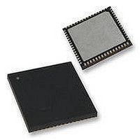
PIC18F65K90-I/MR Microchip Technology, PIC18F65K90-I/MR Datasheet - Page 189

PIC18F65K90-I/MR
Manufacturer Part Number
PIC18F65K90-I/MR
Description
32kB Flash, 2kB RAM, 1kB EE, NanoWatt XLP, LCD 64 QFN 9x9x0.9mm TUBE
Manufacturer
Microchip Technology
Series
PIC® XLP™ 18Fr
Datasheet
1.PIC18F65K90-IMR.pdf
(570 pages)
Specifications of PIC18F65K90-I/MR
Processor Series
PIC18F
Core
PIC
Data Bus Width
8 bit
Program Memory Type
Flash
Program Memory Size
32 KB
Data Ram Size
2 KB
Interface Type
I2C, SPI
Maximum Clock Frequency
64 MHz
Number Of Timers
8
Operating Supply Voltage
1.8 V to 5.5 V
Maximum Operating Temperature
+ 125 C
3rd Party Development Tools
52715-96, 52716-328, 52717-734, 52712-325, EWPIC18
Minimum Operating Temperature
- 40 C
On-chip Adc
12 bit, 16 Channel
Core Processor
PIC
Core Size
8-Bit
Speed
64MHz
Connectivity
I²C, LIN, SPI, UART/USART
Peripherals
Brown-out Detect/Reset, LCD, POR, PWM, WDT
Number Of I /o
53
Eeprom Size
1K x 8
Ram Size
2K x 8
Voltage - Supply (vcc/vdd)
1.8 V ~ 5.5 V
Data Converters
A/D 16x12b
Oscillator Type
Internal
Operating Temperature
-40°C ~ 85°C
Package / Case
64-VFQFN Exposed Pad
Lead Free Status / Rohs Status
Details
- Current page: 189 of 570
- Download datasheet (5Mb)
13.2
The Timer1 module is an 8 or 16-bit incrementing
counter that is accessed through the TMR1H:TMR1L
register pair.
When used with an internal clock source, the module is
a timer and increments on every instruction cycle.
When used with an external clock source, the module
can be used as either a timer or counter. It increments
on every selected edge of the external source.
Timer1 is enabled by configuring the TMR1ON and
TMR1GE bits in the T1CON and T1GCON registers,
respectively.
When SOSC is selected as a Crystal mode (by
SOSCEL), the RC1/SOSCI/ECCP2/P2A/SEG32 and
RC0/SOSCO/SCLKI pins become inputs. This means
the values of TRISC<1:0> are ignored and the pins are
read as ‘0’.
13.3
The TMR1CS<1:0> and SOSCEN bits of the T1CON
register are used to select the clock source for Timer1.
Register 13-1
13.3.1
When the internal clock source is selected, the
TMR1H:TMR1L register pair will increment on multiples
of F
TABLE 13-1:
2009-2011 Microchip Technology Inc.
OSC
TMR1CS1
, as determined by the Timer1 prescaler.
Timer1 Operation
Clock Source Selection
0
0
1
1
INTERNAL CLOCK SOURCE
displays the clock source selections.
TIMER1 CLOCK SOURCE SELECTION
TMR1CS0
1
0
0
0
SOSCEN
x
x
0
1
PIC18F87K90 FAMILY
Clock Source (F
Instruction Clock (F
External Clock on T1CKI Pin
Oscillator Circuit on SOSCI/SOSCO Pins
13.3.2
When the external clock source is selected, the Timer1
module may work as a timer or a counter.
When enabled to count, Timer1 is incremented on the
rising edge of the external clock input, T1CKI. Either of
these external clock sources can be synchronized to the
microcontroller
asynchronously.
When used as a timer with a clock oscillator, an
external, 32.768 kHz crystal can be used in conjunction
with the dedicated internal oscillator circuit.
Note:
EXTERNAL CLOCK SOURCE
In Counter mode, a falling edge must be
registered by the counter prior to the first
incrementing rising edge after any one or
more of the following conditions:
• Timer1 is enabled after a POR Reset
• Write to TMR1H or TMR1L
• Timer1 is disabled
• Timer1 is disabled (TMR1ON = 0)
When T1CKI is high, Timer1 is enabled
(TMR1ON = 1) when T1CKI is low.
OSC
system
OSC
Clock Source
)
/4)
clock
or
DS39957D-page 189
they
can
run
Related parts for PIC18F65K90-I/MR
Image
Part Number
Description
Manufacturer
Datasheet
Request
R

Part Number:
Description:
Manufacturer:
Microchip Technology Inc.
Datasheet:

Part Number:
Description:
Manufacturer:
Microchip Technology Inc.
Datasheet:

Part Number:
Description:
Manufacturer:
Microchip Technology Inc.
Datasheet:

Part Number:
Description:
Manufacturer:
Microchip Technology Inc.
Datasheet:

Part Number:
Description:
Manufacturer:
Microchip Technology Inc.
Datasheet:

Part Number:
Description:
Manufacturer:
Microchip Technology Inc.
Datasheet:

Part Number:
Description:
Manufacturer:
Microchip Technology Inc.
Datasheet:

Part Number:
Description:
Manufacturer:
Microchip Technology Inc.
Datasheet:


