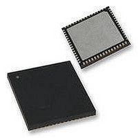
PIC18F65K90-I/MR Microchip Technology, PIC18F65K90-I/MR Datasheet - Page 194

PIC18F65K90-I/MR
Manufacturer Part Number
PIC18F65K90-I/MR
Description
32kB Flash, 2kB RAM, 1kB EE, NanoWatt XLP, LCD 64 QFN 9x9x0.9mm TUBE
Manufacturer
Microchip Technology
Series
PIC® XLP™ 18Fr
Datasheet
1.PIC18F65K90-IMR.pdf
(570 pages)
Specifications of PIC18F65K90-I/MR
Processor Series
PIC18F
Core
PIC
Data Bus Width
8 bit
Program Memory Type
Flash
Program Memory Size
32 KB
Data Ram Size
2 KB
Interface Type
I2C, SPI
Maximum Clock Frequency
64 MHz
Number Of Timers
8
Operating Supply Voltage
1.8 V to 5.5 V
Maximum Operating Temperature
+ 125 C
3rd Party Development Tools
52715-96, 52716-328, 52717-734, 52712-325, EWPIC18
Minimum Operating Temperature
- 40 C
On-chip Adc
12 bit, 16 Channel
Core Processor
PIC
Core Size
8-Bit
Speed
64MHz
Connectivity
I²C, LIN, SPI, UART/USART
Peripherals
Brown-out Detect/Reset, LCD, POR, PWM, WDT
Number Of I /o
53
Eeprom Size
1K x 8
Ram Size
2K x 8
Voltage - Supply (vcc/vdd)
1.8 V ~ 5.5 V
Data Converters
A/D 16x12b
Oscillator Type
Internal
Operating Temperature
-40°C ~ 85°C
Package / Case
64-VFQFN Exposed Pad
Lead Free Status / Rohs Status
Details
- Current page: 194 of 570
- Download datasheet (5Mb)
PIC18F87K90 FAMILY
13.8.2
The Timer1 gate source can be selected from one of
four sources. Source selection is controlled by the
T1GSSx bits, T1GCON<1:0> (see
TABLE 13-4:
The polarity for each available source is also selectable,
controlled by the T1GPOL bit (T1GCON<6>).
13.8.2.1
The T1G pin is one source for Timer1 gate control. It
can be used to supply an external source to the Timer1
gate circuitry.
DS39957D-page 194
T1GSS<1:0>
00
01
10
11
TIMER1 GATE SOURCE
SELECTION
T1G Pin Gate Operation
Timer1 Gate Pin
TMR2 to Match PR2
(TMR2 increments to match PR2)
Comparator 1 Output
(Comparator logic high output)
Comparator 2 Output
(Comparator logic high output)
TIMER1 GATE SOURCES
Timer1 Gate Source
Table
13-4).
13.8.2.2
The TMR2 register will increment until it matches the
value in the PR2 register. On the very next increment
cycle, TMR2 will be reset to 00h. When this Reset
occurs, a low-to-high pulse will automatically be gener-
ated and internally supplied to the Timer1 gate circuitry.
The pulse will remain high for one instruction cycle and
will return back to a low state until the next match.
Depending on T1GPOL, Timer1 increments differently
when TMR2 matches PR2. When T1GPOL = 1, Timer1
increments for a single instruction cycle following a
TMR2 match with PR2. When T1GPOL = 0, Timer1
increments continuously, except for the cycle following
the match, when the gate signal goes from low-to-high.
13.8.2.3
The output of Comparator 1 can be internally supplied
to the Timer1 gate circuitry. After setting up
Comparator 1 with the CM1CON register, Timer1 will
increment depending on the transition of the
CMP1OUT (CMSTAT<5>) bit.
13.8.2.4
The output of Comparator 2 can be internally supplied
to the Timer1 gate circuitry. After setting up
Comparator 2 with the CM2CON register, Timer1 will
increment depending on the transition of the
CMP2OUT (CMSTAT<6>) bit.
Timer2 Match Gate Operation
Comparator 1 Output Gate Operation
Comparator 2 Output Gate Operation
2009-2011 Microchip Technology Inc.
Related parts for PIC18F65K90-I/MR
Image
Part Number
Description
Manufacturer
Datasheet
Request
R

Part Number:
Description:
Manufacturer:
Microchip Technology Inc.
Datasheet:

Part Number:
Description:
Manufacturer:
Microchip Technology Inc.
Datasheet:

Part Number:
Description:
Manufacturer:
Microchip Technology Inc.
Datasheet:

Part Number:
Description:
Manufacturer:
Microchip Technology Inc.
Datasheet:

Part Number:
Description:
Manufacturer:
Microchip Technology Inc.
Datasheet:

Part Number:
Description:
Manufacturer:
Microchip Technology Inc.
Datasheet:

Part Number:
Description:
Manufacturer:
Microchip Technology Inc.
Datasheet:

Part Number:
Description:
Manufacturer:
Microchip Technology Inc.
Datasheet:


