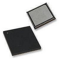
PIC18F65K90-I/MR Microchip Technology, PIC18F65K90-I/MR Datasheet - Page 193

PIC18F65K90-I/MR
Manufacturer Part Number
PIC18F65K90-I/MR
Description
32kB Flash, 2kB RAM, 1kB EE, NanoWatt XLP, LCD 64 QFN 9x9x0.9mm TUBE
Manufacturer
Microchip Technology
Series
PIC® XLP™ 18Fr
Datasheet
1.PIC18F65K90-IMR.pdf
(570 pages)
Specifications of PIC18F65K90-I/MR
Processor Series
PIC18F
Core
PIC
Data Bus Width
8 bit
Program Memory Type
Flash
Program Memory Size
32 KB
Data Ram Size
2 KB
Interface Type
I2C, SPI
Maximum Clock Frequency
64 MHz
Number Of Timers
8
Operating Supply Voltage
1.8 V to 5.5 V
Maximum Operating Temperature
+ 125 C
3rd Party Development Tools
52715-96, 52716-328, 52717-734, 52712-325, EWPIC18
Minimum Operating Temperature
- 40 C
On-chip Adc
12 bit, 16 Channel
Core Processor
PIC
Core Size
8-Bit
Speed
64MHz
Connectivity
I²C, LIN, SPI, UART/USART
Peripherals
Brown-out Detect/Reset, LCD, POR, PWM, WDT
Number Of I /o
53
Eeprom Size
1K x 8
Ram Size
2K x 8
Voltage - Supply (vcc/vdd)
1.8 V ~ 5.5 V
Data Converters
A/D 16x12b
Oscillator Type
Internal
Operating Temperature
-40°C ~ 85°C
Package / Case
64-VFQFN Exposed Pad
Lead Free Status / Rohs Status
Details
- Current page: 193 of 570
- Download datasheet (5Mb)
13.7
If ECCP modules are configured to use Timer1 and to
generate a Special Event Trigger in Compare mode
(CCPxM<3:0> = 1011), this signal will reset Timer1. The
trigger from ECCP2 will also start an A/D conversion, if
the A/D module is enabled. (For more information, see
Section 19.3.4 “Special Event
To take advantage of this feature, the module must be
configured as either a timer or a synchronous counter.
When used this way, the CCPRxH:CCPRxL register
pair effectively becomes a Period register for Timer1.
If Timer1 is running in Asynchronous Counter mode,
this Reset operation may not work.
In the event that a write to Timer1 coincides with a
Special Event Trigger, the write operation will take
precedence.
13.8
Timer1 can be configured to count freely or the count can
be enabled and disabled using the Timer1 gate circuitry.
This is also referred to as Timer1 gate count enable.
Timer1 gate can also be driven by multiple selectable
sources.
FIGURE 13-4:
2009-2011 Microchip Technology Inc.
Note:
TMR1GE
T1GPOL
T1GVAL
T1G_IN
Resetting Timer1 Using the ECCP
Special Event Trigger
Timer1 Gate
Timer1
T1CKI
The Special Event Trigger from the
ECCPx module will only clear the TMR1
register’s content, but not set the TMR1IF
interrupt flag bit (PIR1<0>).
TIMER1 GATE COUNT ENABLE MODE
N
Trigger”.)
N + 1
PIC18F87K90 FAMILY
13.8.1
The Timer1 Gate Enable mode is enabled by setting
the TMR1GE bit of the T1GCON register. The polarity
of the Timer1 Gate Enable mode is configured using
the T1GPOL bit (T1GCON<6>).
When Timer1 Gate Enable mode is enabled, Timer1
will increment on the rising edge of the Timer1 clock
source. When Timer1 Gate Enable mode is disabled,
no incrementing will occur and Timer1 will hold the
current count. See
TABLE 13-3:
† The clock on which TMR1 is running. For more
T1CLK
Note:
information, see
(†)
N + 2
(T1GCON<6>)
TIMER1 GATE COUNT ENABLE
The CCP and ECCP modules use Timers,
1 through 8, for some modes. The assign-
ment of a particular timer to a CCP/ECCP
module is determined by the Timer to CCP
enable bits in the CCPTMRSx registers.
For more details, see
Register 18-3
T1GPOL
0
0
1
1
TIMER1 GATE ENABLE
SELECTIONS
Figure
Figure 13-4
13-1.
T1G Pin
and
0
1
0
1
N + 3
Register 19-2
for timing details.
Counts
Holds Count
Holds Count
Counts
DS39957D-page 193
Timer1 Operation
N + 4
Register
18-2,
Related parts for PIC18F65K90-I/MR
Image
Part Number
Description
Manufacturer
Datasheet
Request
R

Part Number:
Description:
Manufacturer:
Microchip Technology Inc.
Datasheet:

Part Number:
Description:
Manufacturer:
Microchip Technology Inc.
Datasheet:

Part Number:
Description:
Manufacturer:
Microchip Technology Inc.
Datasheet:

Part Number:
Description:
Manufacturer:
Microchip Technology Inc.
Datasheet:

Part Number:
Description:
Manufacturer:
Microchip Technology Inc.
Datasheet:

Part Number:
Description:
Manufacturer:
Microchip Technology Inc.
Datasheet:

Part Number:
Description:
Manufacturer:
Microchip Technology Inc.
Datasheet:

Part Number:
Description:
Manufacturer:
Microchip Technology Inc.
Datasheet:


