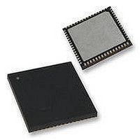
PIC18F65K90-I/MR Microchip Technology, PIC18F65K90-I/MR Datasheet - Page 166

PIC18F65K90-I/MR
Manufacturer Part Number
PIC18F65K90-I/MR
Description
32kB Flash, 2kB RAM, 1kB EE, NanoWatt XLP, LCD 64 QFN 9x9x0.9mm TUBE
Manufacturer
Microchip Technology
Series
PIC® XLP™ 18Fr
Datasheet
1.PIC18F65K90-IMR.pdf
(570 pages)
Specifications of PIC18F65K90-I/MR
Processor Series
PIC18F
Core
PIC
Data Bus Width
8 bit
Program Memory Type
Flash
Program Memory Size
32 KB
Data Ram Size
2 KB
Interface Type
I2C, SPI
Maximum Clock Frequency
64 MHz
Number Of Timers
8
Operating Supply Voltage
1.8 V to 5.5 V
Maximum Operating Temperature
+ 125 C
3rd Party Development Tools
52715-96, 52716-328, 52717-734, 52712-325, EWPIC18
Minimum Operating Temperature
- 40 C
On-chip Adc
12 bit, 16 Channel
Core Processor
PIC
Core Size
8-Bit
Speed
64MHz
Connectivity
I²C, LIN, SPI, UART/USART
Peripherals
Brown-out Detect/Reset, LCD, POR, PWM, WDT
Number Of I /o
53
Eeprom Size
1K x 8
Ram Size
2K x 8
Voltage - Supply (vcc/vdd)
1.8 V ~ 5.5 V
Data Converters
A/D 16x12b
Oscillator Type
Internal
Operating Temperature
-40°C ~ 85°C
Package / Case
64-VFQFN Exposed Pad
Lead Free Status / Rohs Status
Details
- Current page: 166 of 570
- Download datasheet (5Mb)
corresponding Data Direction and Output Latch registers
PIC18F87K90 FAMILY
11.5
PORTD is an 8-bit wide, bidirectional port. The
are TRISD and LATD.
All pins on PORTD are implemented with Schmitt
Trigger input buffers. Each pin is individually
configurable as an input or output.
Each of the PORTD pins has a weak internal pull-up. A
single control bit can turn off all the pull-ups. This is
performed by clearing bit, RDPU (PADCFG1<7>). The
weak pull-up is automatically turned off when the port
pin is configured as an output. The pull-ups are
disabled on all device Resets.
All of the PORTD pins are multiplexed with LCD
segment drives that are controlled by bits in the
LCDSE0 register. RD0 is multiplexed with the CTMU
pulse generator output.
DS39957D-page 166
Note:
PORTD, TRISD and
LATD Registers
These pins are configured as digital inputs
on any device Reset.
RD0 has a CTMU functionality. RD1 has the functionality
I/O port functionality is only available when the LCD
segments are disabled.
The PORTD also has the I
RD4, RD5 and RD6. The pins for SPI are also configu-
rable for open-drain output. Open-drain configuration is
selected by setting the SSPxOD control bits in the
ODCON1 register.
for a Timer5 clock input and also Timer7 has functionality
for an external clock gate input.
EXAMPLE 11-4:
CLRF
CLRF
MOVLW
MOVWF
PORTD
LATD
0CFh
TRISD
2009-2011 Microchip Technology Inc.
; Initialize PORTD by
; clearing output
; data latches
; Alternate method
; to clear output
; data latches
; Value used to
; initialize data
; direction
; Set RD<3:0> as inputs
; RD<5:4> as outputs
; RD<7:6> as inputs
INITIALIZING PORTD
2
C and SPI functionality on
Related parts for PIC18F65K90-I/MR
Image
Part Number
Description
Manufacturer
Datasheet
Request
R

Part Number:
Description:
Manufacturer:
Microchip Technology Inc.
Datasheet:

Part Number:
Description:
Manufacturer:
Microchip Technology Inc.
Datasheet:

Part Number:
Description:
Manufacturer:
Microchip Technology Inc.
Datasheet:

Part Number:
Description:
Manufacturer:
Microchip Technology Inc.
Datasheet:

Part Number:
Description:
Manufacturer:
Microchip Technology Inc.
Datasheet:

Part Number:
Description:
Manufacturer:
Microchip Technology Inc.
Datasheet:

Part Number:
Description:
Manufacturer:
Microchip Technology Inc.
Datasheet:

Part Number:
Description:
Manufacturer:
Microchip Technology Inc.
Datasheet:


