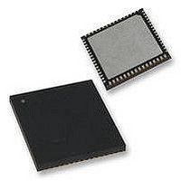
PIC18F65K90-I/MR Microchip Technology, PIC18F65K90-I/MR Datasheet - Page 387

PIC18F65K90-I/MR
Manufacturer Part Number
PIC18F65K90-I/MR
Description
32kB Flash, 2kB RAM, 1kB EE, NanoWatt XLP, LCD 64 QFN 9x9x0.9mm TUBE
Manufacturer
Microchip Technology
Series
PIC® XLP™ 18Fr
Datasheet
1.PIC18F65K90-IMR.pdf
(570 pages)
Specifications of PIC18F65K90-I/MR
Processor Series
PIC18F
Core
PIC
Data Bus Width
8 bit
Program Memory Type
Flash
Program Memory Size
32 KB
Data Ram Size
2 KB
Interface Type
I2C, SPI
Maximum Clock Frequency
64 MHz
Number Of Timers
8
Operating Supply Voltage
1.8 V to 5.5 V
Maximum Operating Temperature
+ 125 C
3rd Party Development Tools
52715-96, 52716-328, 52717-734, 52712-325, EWPIC18
Minimum Operating Temperature
- 40 C
On-chip Adc
12 bit, 16 Channel
Core Processor
PIC
Core Size
8-Bit
Speed
64MHz
Connectivity
I²C, LIN, SPI, UART/USART
Peripherals
Brown-out Detect/Reset, LCD, POR, PWM, WDT
Number Of I /o
53
Eeprom Size
1K x 8
Ram Size
2K x 8
Voltage - Supply (vcc/vdd)
1.8 V ~ 5.5 V
Data Converters
A/D 16x12b
Oscillator Type
Internal
Operating Temperature
-40°C ~ 85°C
Package / Case
64-VFQFN Exposed Pad
Lead Free Status / Rohs Status
Details
- Current page: 387 of 570
- Download datasheet (5Mb)
23.8
A/D conversion can be started by the Special Event
Trigger of any of these modules:
• ECCP2 – Requires CCP2M<3:0> bits
• CTMU – Requires the setting of the CTTRIG bit
• Timer1
• RTCC
To start an A/D conversion:
• The A/D module must be enabled (ADON = 1 )
• The appropriate analog input channel is selected
• The minimum acquisition period is set in one of
With these conditions met, the trigger sets the
GO/DONE bit and the A/D acquisition starts.
If the A/D module is not enabled (ADON = 0 ), the
module ignores the Special Event Trigger.
2009-2011 Microchip Technology Inc.
(CCP2CON<3:0>) set at ‘ 1011 ’
(CTMUCONH<0>)
these ways:
- Timing provided by the user
- Selection made of an appropriate T
Note:
Use of the Special Event Triggers
With an ECCP2 trigger, Timer1 or Timer3
is cleared. The timers reset to automati-
cally repeat the A/D acquisition period
with minimal software overhead (moving
ADRESH:ADRESL to the desired loca-
tion). If the A/D module is not enabled, the
Special Event Trigger is ignored by the
module, but the timer’s counter resets.
ACQ
time
PIC18F87K90 FAMILY
23.9
The selection of the automatic acquisition time and A/D
conversion clock is determined, in part, by the clock
source and frequency while in a power-managed
mode.
If the A/D is expected to operate while the device is in
a power-managed mode, the ACQT<2:0> and
ADCS<2:0> bits in ADCON2 should be updated in
accordance with the power-managed mode clock that
will be used.
After the power-managed mode is entered (either of the
power-managed Run modes), an A/D acquisition or
conversion may be started. Once an acquisition or
conversion is started, the device should continue to be
clocked by the same power-managed mode clock source
until the conversion has been completed. If desired, the
device
power-managed Idle mode during the conversion.
If the power-managed mode clock frequency is less
than 1 MHz, the A/D RC clock source should be
selected.
Operation in Sleep mode requires that the A/D RC
clock be selected. If bits, ACQT<2:0>, are set to ‘ 000 ’
and a conversion is started, the conversion will be
delayed one instruction cycle to allow execution of the
SLEEP instruction and entry into Sleep mode. The
IDLEN and SCS<1:0> bits in the OSCCON register
must have already been cleared prior to starting the
conversion.
may
Operation in Power-Managed
Modes
be
placed
into the
DS39957D-page 387
corresponding
Related parts for PIC18F65K90-I/MR
Image
Part Number
Description
Manufacturer
Datasheet
Request
R

Part Number:
Description:
Manufacturer:
Microchip Technology Inc.
Datasheet:

Part Number:
Description:
Manufacturer:
Microchip Technology Inc.
Datasheet:

Part Number:
Description:
Manufacturer:
Microchip Technology Inc.
Datasheet:

Part Number:
Description:
Manufacturer:
Microchip Technology Inc.
Datasheet:

Part Number:
Description:
Manufacturer:
Microchip Technology Inc.
Datasheet:

Part Number:
Description:
Manufacturer:
Microchip Technology Inc.
Datasheet:

Part Number:
Description:
Manufacturer:
Microchip Technology Inc.
Datasheet:

Part Number:
Description:
Manufacturer:
Microchip Technology Inc.
Datasheet:


