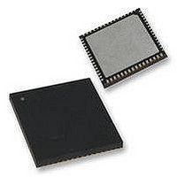
PIC18F65K90-I/MR Microchip Technology, PIC18F65K90-I/MR Datasheet - Page 334

PIC18F65K90-I/MR
Manufacturer Part Number
PIC18F65K90-I/MR
Description
32kB Flash, 2kB RAM, 1kB EE, NanoWatt XLP, LCD 64 QFN 9x9x0.9mm TUBE
Manufacturer
Microchip Technology
Series
PIC® XLP™ 18Fr
Datasheet
1.PIC18F65K90-IMR.pdf
(570 pages)
Specifications of PIC18F65K90-I/MR
Processor Series
PIC18F
Core
PIC
Data Bus Width
8 bit
Program Memory Type
Flash
Program Memory Size
32 KB
Data Ram Size
2 KB
Interface Type
I2C, SPI
Maximum Clock Frequency
64 MHz
Number Of Timers
8
Operating Supply Voltage
1.8 V to 5.5 V
Maximum Operating Temperature
+ 125 C
3rd Party Development Tools
52715-96, 52716-328, 52717-734, 52712-325, EWPIC18
Minimum Operating Temperature
- 40 C
On-chip Adc
12 bit, 16 Channel
Core Processor
PIC
Core Size
8-Bit
Speed
64MHz
Connectivity
I²C, LIN, SPI, UART/USART
Peripherals
Brown-out Detect/Reset, LCD, POR, PWM, WDT
Number Of I /o
53
Eeprom Size
1K x 8
Ram Size
2K x 8
Voltage - Supply (vcc/vdd)
1.8 V ~ 5.5 V
Data Converters
A/D 16x12b
Oscillator Type
Internal
Operating Temperature
-40°C ~ 85°C
Package / Case
64-VFQFN Exposed Pad
Lead Free Status / Rohs Status
Details
- Current page: 334 of 570
- Download datasheet (5Mb)
PIC18F87K90 FAMILY
21.4.6.1
The master device generates all of the serial clock
pulses and the Start and Stop conditions. A transfer is
ended with a Stop condition or with a Repeated Start
condition. Since the Repeated Start condition is also
the beginning of the next serial transfer, the I
not be released.
In Master Transmitter mode, serial data is output
through SDAx while SCLx outputs the serial clock. The
first byte transmitted contains the slave address of the
receiving device (7 bits) and the Read/Write (R/W) bit.
In this case, the R/W bit will be logic ‘0’. Serial data is
transmitted, 8 bits at a time. After each byte is transmit-
ted, an Acknowledge bit is received. Start and Stop
conditions are output to indicate the beginning and the
end of a serial transfer.
In Master Receive mode, the first byte transmitted
contains the slave address of the transmitting device
(7 bits) and the R/W bit. In this case, the R/W bit will be
logic ‘1’. Thus, the first byte transmitted is a 7-bit slave
address, followed by a ‘1’ to indicate the receive bit.
Serial data is received via SDAx, while SCLx outputs
the serial clock. Serial data is received, 8 bits at a time.
After each byte is received, an Acknowledge bit is
transmitted. Start and Stop conditions indicate the
beginning and end of transmission.
The Baud Rate Generator, used for the SPI mode
operation, is used to set the SCLx clock frequency for
either 100 kHz, 400 kHz or 1 MHz I
Section 21.4.7 “Baud Rate”
DS39957D-page 334
I
2
C Master Mode Operation
for more details.
2
C operation. See
2
C bus will
A typical transmit sequence would go as follows:
1.
2.
3.
4.
5.
6.
7.
8.
9.
10. The MSSPx module generates an interrupt at
11. The user generates a Stop condition by setting
12. An interrupt is generated once the Stop condition
The user generates a Start condition by setting
the Start Enable bit, SEN (SSPxCON2<0>).
SSPxIF is set. The MSSPx module will wait the
required start time before any other operation
takes place.
The user loads the SSPxBUF with the slave
address to transmit.
Address is shifted out the SDAx pin until all 8 bits
are transmitted.
The MSSPx module shifts in the ACK bit from
the slave device and writes its value into the
SSPxCON2 register (SSPxCON2<6>).
The MSSPx module generates an interrupt at
the end of the ninth clock cycle by setting the
SSPxIF bit.
The user loads the SSPxBUF with 8 bits of data.
Data is shifted out the SDAx pin until all 8 bits
are transmitted.
The MSSPx module shifts in the ACK bit from
the slave device and writes its value into the
SSPxCON2 register (SSPxCON2<6>).
the end of the ninth clock cycle by setting the
SSPxIF bit.
the Stop Enable bit, PEN (SSPxCON2<2>).
is complete.
2009-2011 Microchip Technology Inc.
Related parts for PIC18F65K90-I/MR
Image
Part Number
Description
Manufacturer
Datasheet
Request
R

Part Number:
Description:
Manufacturer:
Microchip Technology Inc.
Datasheet:

Part Number:
Description:
Manufacturer:
Microchip Technology Inc.
Datasheet:

Part Number:
Description:
Manufacturer:
Microchip Technology Inc.
Datasheet:

Part Number:
Description:
Manufacturer:
Microchip Technology Inc.
Datasheet:

Part Number:
Description:
Manufacturer:
Microchip Technology Inc.
Datasheet:

Part Number:
Description:
Manufacturer:
Microchip Technology Inc.
Datasheet:

Part Number:
Description:
Manufacturer:
Microchip Technology Inc.
Datasheet:

Part Number:
Description:
Manufacturer:
Microchip Technology Inc.
Datasheet:


