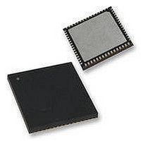
PIC18F65K90-I/MR Microchip Technology, PIC18F65K90-I/MR Datasheet - Page 321

PIC18F65K90-I/MR
Manufacturer Part Number
PIC18F65K90-I/MR
Description
32kB Flash, 2kB RAM, 1kB EE, NanoWatt XLP, LCD 64 QFN 9x9x0.9mm TUBE
Manufacturer
Microchip Technology
Series
PIC® XLP™ 18Fr
Datasheet
1.PIC18F65K90-IMR.pdf
(570 pages)
Specifications of PIC18F65K90-I/MR
Processor Series
PIC18F
Core
PIC
Data Bus Width
8 bit
Program Memory Type
Flash
Program Memory Size
32 KB
Data Ram Size
2 KB
Interface Type
I2C, SPI
Maximum Clock Frequency
64 MHz
Number Of Timers
8
Operating Supply Voltage
1.8 V to 5.5 V
Maximum Operating Temperature
+ 125 C
3rd Party Development Tools
52715-96, 52716-328, 52717-734, 52712-325, EWPIC18
Minimum Operating Temperature
- 40 C
On-chip Adc
12 bit, 16 Channel
Core Processor
PIC
Core Size
8-Bit
Speed
64MHz
Connectivity
I²C, LIN, SPI, UART/USART
Peripherals
Brown-out Detect/Reset, LCD, POR, PWM, WDT
Number Of I /o
53
Eeprom Size
1K x 8
Ram Size
2K x 8
Voltage - Supply (vcc/vdd)
1.8 V ~ 5.5 V
Data Converters
A/D 16x12b
Oscillator Type
Internal
Operating Temperature
-40°C ~ 85°C
Package / Case
64-VFQFN Exposed Pad
Lead Free Status / Rohs Status
Details
- Current page: 321 of 570
- Download datasheet (5Mb)
21.4.3.5
When the R/W bit of the address byte is clear and an
address match occurs, the R/W bit of the SSPxSTAT
register is cleared. The received address is loaded into
the SSPxBUF register and the SDAx line is held low
(ACK).
When the address byte overflow condition exists, then
the no Acknowledge (ACK) pulse is given. An overflow
condition is defined as either bit, BF (SSPxSTAT<0>),
is set or bit, SSPOV (SSPxCON1<6>), is set.
An MSSP interrupt is generated for each data transfer
byte. The interrupt flag bit, SSPxIF, must be cleared in
software. The SSPxSTAT register is used to determine
the status of the byte.
If SEN is enabled (SSPxCON2<0> = 1), SCLx will be
held low (clock stretch) following each data transfer. The
clock must be released by setting bit, CKP
(SSPxCON1<4>).
Stretching”
2009-2011 Microchip Technology Inc.
for more details.
Reception
See
Section 21.4.4
“Clock
PIC18F87K90 FAMILY
21.4.3.6
When the R/W bit of the incoming address byte is set
and an address match occurs, the R/W bit of the
SSPxSTAT register is set. The received address is
loaded into the SSPxBUF register. The ACK pulse will
be sent on the ninth bit and pin, SCLx, is held low
regardless of SEN (see
Stretching”
the master will be unable to assert another clock pulse
until the slave is done preparing the transmit data. The
transmit data must be loaded into the SSPxBUF regis-
ter which also loads the SSPxSR register. Then, pin,
SCLx, should be enabled by setting bit, CKP
(SSPxCON1<4>). The eight data bits are shifted out on
the falling edge of the SCLx input. This ensures that the
SDAx signal is valid during the SCLx high time
(Figure
The ACK pulse from the master-receiver is latched on
the rising edge of the ninth SCLx input pulse. If the
SDAx line is high (not ACK), then the data transfer is
complete. In this case, when the ACK is latched by the
slave, the slave logic is reset and the slave monitors for
another occurrence of the Start bit. If the SDAx line was
low (ACK), the next transmit data must be loaded into
the SSPxBUF register. Again, pin, SCLx, must be
enabled by setting bit, CKP.
An MSSP interrupt is generated for each data transfer
byte. The SSPxIF bit must be cleared in software and
the SSPxSTAT register is used to determine the status
of the byte. The SSPxIF bit is set on the falling edge of
the ninth clock pulse.
21-10).
for more details). By stretching the clock,
Transmission
Section 21.4.4 “Clock
DS39957D-page 321
Related parts for PIC18F65K90-I/MR
Image
Part Number
Description
Manufacturer
Datasheet
Request
R

Part Number:
Description:
Manufacturer:
Microchip Technology Inc.
Datasheet:

Part Number:
Description:
Manufacturer:
Microchip Technology Inc.
Datasheet:

Part Number:
Description:
Manufacturer:
Microchip Technology Inc.
Datasheet:

Part Number:
Description:
Manufacturer:
Microchip Technology Inc.
Datasheet:

Part Number:
Description:
Manufacturer:
Microchip Technology Inc.
Datasheet:

Part Number:
Description:
Manufacturer:
Microchip Technology Inc.
Datasheet:

Part Number:
Description:
Manufacturer:
Microchip Technology Inc.
Datasheet:

Part Number:
Description:
Manufacturer:
Microchip Technology Inc.
Datasheet:


