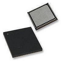
PIC18F65K90-I/MR Microchip Technology, PIC18F65K90-I/MR Datasheet - Page 543

PIC18F65K90-I/MR
Manufacturer Part Number
PIC18F65K90-I/MR
Description
32kB Flash, 2kB RAM, 1kB EE, NanoWatt XLP, LCD 64 QFN 9x9x0.9mm TUBE
Manufacturer
Microchip Technology
Series
PIC® XLP™ 18Fr
Datasheet
1.PIC18F65K90-IMR.pdf
(570 pages)
Specifications of PIC18F65K90-I/MR
Processor Series
PIC18F
Core
PIC
Data Bus Width
8 bit
Program Memory Type
Flash
Program Memory Size
32 KB
Data Ram Size
2 KB
Interface Type
I2C, SPI
Maximum Clock Frequency
64 MHz
Number Of Timers
8
Operating Supply Voltage
1.8 V to 5.5 V
Maximum Operating Temperature
+ 125 C
3rd Party Development Tools
52715-96, 52716-328, 52717-734, 52712-325, EWPIC18
Minimum Operating Temperature
- 40 C
On-chip Adc
12 bit, 16 Channel
Core Processor
PIC
Core Size
8-Bit
Speed
64MHz
Connectivity
I²C, LIN, SPI, UART/USART
Peripherals
Brown-out Detect/Reset, LCD, POR, PWM, WDT
Number Of I /o
53
Eeprom Size
1K x 8
Ram Size
2K x 8
Voltage - Supply (vcc/vdd)
1.8 V ~ 5.5 V
Data Converters
A/D 16x12b
Oscillator Type
Internal
Operating Temperature
-40°C ~ 85°C
Package / Case
64-VFQFN Exposed Pad
Lead Free Status / Rohs Status
Details
- Current page: 543 of 570
- Download datasheet (5Mb)
FIGURE 31-21:
TABLE 31-26: A/D CONVERSION REQUIREMENTS
2009-2011 Microchip Technology Inc.
130
131
132
135
137
Note 1:
Param
No.
Note 1:
A/D DATA
SAMPLE
A/D CLK
2:
3:
4:
ADRES
BSF ADCON0, GO
T
T
T
T
T
Symbol
ADIF
AD
CNV
ACQ
SWC
DIS
2:
GO
Q4
The time of the A/D clock period is dependent on the device frequency and the T
ADRES registers may be read on the following T
The time for the holding capacitor to acquire the “New” input voltage when the voltage changes full scale
after the conversion (V
On the following cycle of the device clock.
If the A/D clock source is selected as RC, a time of T
be executed.
This is a minimal RC delay (typically 100 ns), which also disconnects the holding capacitor from the analog input.
132
A/D Clock Period
Conversion Time
(not including acquisition time)
Acquisition Time
Switching Time from Convert Sample
Discharge Time
A/D CONVERSION TIMING
(Note 2)
Characteristic
DD
11
(3)
to V
10
SS
or V
OLD_DATA
9
SS
(2)
to V
. . .
SAMPLING STOPPED
CY
DD
is added before the A/D clock starts. This allows the SLEEP instruction to
). The source impedance ( R
CY
PIC18F87K90 FAMILY
. . .
131
130
cycle.
Min
0.8
1.4
1.4
0.2
14
—
—
—
2
(Note 4)
12.5
25
Max
15
—
—
1
3
1
(1)
(1)
Units
T
s
s
s
s
s
s
AD
S
0
) on the input channels is 50 .
T
V
V
A/D RC mode
V
-40 C to +125 C
OSC
REF
DD
DD
AD
= 3.0V; T
= 3.0V; A/D RC mode
based, V
full range
clock divider.
NEW_DATA
DONE
Conditions
DS39957D-page 543
T
CY
OSC
REF
(Note 1)
based,
3.0V
Related parts for PIC18F65K90-I/MR
Image
Part Number
Description
Manufacturer
Datasheet
Request
R

Part Number:
Description:
Manufacturer:
Microchip Technology Inc.
Datasheet:

Part Number:
Description:
Manufacturer:
Microchip Technology Inc.
Datasheet:

Part Number:
Description:
Manufacturer:
Microchip Technology Inc.
Datasheet:

Part Number:
Description:
Manufacturer:
Microchip Technology Inc.
Datasheet:

Part Number:
Description:
Manufacturer:
Microchip Technology Inc.
Datasheet:

Part Number:
Description:
Manufacturer:
Microchip Technology Inc.
Datasheet:

Part Number:
Description:
Manufacturer:
Microchip Technology Inc.
Datasheet:

Part Number:
Description:
Manufacturer:
Microchip Technology Inc.
Datasheet:


