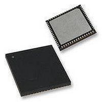
PIC18F65K90-I/MR Microchip Technology, PIC18F65K90-I/MR Datasheet - Page 248

PIC18F65K90-I/MR
Manufacturer Part Number
PIC18F65K90-I/MR
Description
32kB Flash, 2kB RAM, 1kB EE, NanoWatt XLP, LCD 64 QFN 9x9x0.9mm TUBE
Manufacturer
Microchip Technology
Series
PIC® XLP™ 18Fr
Datasheet
1.PIC18F65K90-IMR.pdf
(570 pages)
Specifications of PIC18F65K90-I/MR
Processor Series
PIC18F
Core
PIC
Data Bus Width
8 bit
Program Memory Type
Flash
Program Memory Size
32 KB
Data Ram Size
2 KB
Interface Type
I2C, SPI
Maximum Clock Frequency
64 MHz
Number Of Timers
8
Operating Supply Voltage
1.8 V to 5.5 V
Maximum Operating Temperature
+ 125 C
3rd Party Development Tools
52715-96, 52716-328, 52717-734, 52712-325, EWPIC18
Minimum Operating Temperature
- 40 C
On-chip Adc
12 bit, 16 Channel
Core Processor
PIC
Core Size
8-Bit
Speed
64MHz
Connectivity
I²C, LIN, SPI, UART/USART
Peripherals
Brown-out Detect/Reset, LCD, POR, PWM, WDT
Number Of I /o
53
Eeprom Size
1K x 8
Ram Size
2K x 8
Voltage - Supply (vcc/vdd)
1.8 V ~ 5.5 V
Data Converters
A/D 16x12b
Oscillator Type
Internal
Operating Temperature
-40°C ~ 85°C
Package / Case
64-VFQFN Exposed Pad
Lead Free Status / Rohs Status
Details
- Current page: 248 of 570
- Download datasheet (5Mb)
PIC18F87K90 FAMILY
A PWM output
and a time that the output stays high (duty cycle). The
frequency of the PWM is the inverse of the period
(1/period).
FIGURE 18-4:
18.4.1
The PWM period is specified by writing to the PR2
register. The PWM period can be calculated using the
following formula:
EQUATION 18-1:
PWM frequency is defined as 1/[PWM period].
When TMR2 is equal to PR2, the following three events
occur on the next increment cycle:
• TMR2 is cleared
• The CCP4 pin is set
• The PWM duty cycle is latched from CCPR4L into
TABLE 18-6:
DS39957D-page 248
Timer Prescaler (1, 4, 16)
PR2 Value
Maximum Resolution (bits)
(An exception: If PWM duty cycle = 0%, the CCP4
pin will not be set)
CCPR4H
Note:
PWM Period = [(PR2) + 1] • 4 • T
TMR2 = PR2
PWM Frequency
Duty Cycle
PWM PERIOD
The
Section 14.0 “Timer2
used in the determination of the PWM
frequency. The postscaler could be used
to have a servo update rate at a different
frequency than the PWM output.
(Figure
Period
EXAMPLE PWM FREQUENCIES AND RESOLUTIONS AT 40 MHz
TMR2 = Duty Cycle
Timer2
(TMR2 Prescale Value)
PWM OUTPUT
18-4) has a time base (period)
TMR2 = PR2
postscalers
2.44 kHz
Module”) are not
FFh
OSC
16
14
•
(see
9.77 kHz
FFh
12
4
39.06 kHz
18.4.2
The PWM duty cycle is specified by writing to the
CCPR4L register (using CCP4 as an example) and to
the CCP4CON<5:4> bits. Up to 10-bit resolution is avail-
able. The CCPR4L contains the eight MSbs and the
CCP4CON<5:4> bits contain the two LSbs. This 10-bit
value is represented by CCPR4L:CCP4CON<5:4>. The
following equation is used to calculate the PWM duty
cycle in time:
EQUATION 18-2:
CCPR4L and CCP4CON<5:4> can be written to at any
time, but the duty cycle value is not latched into
CCPR4H until after a match between PR2 and TMR2
occurs (that is, the period is complete). In PWM mode,
CCPR4H is a read-only register.
The CCPR4H register and a 2-bit internal latch are
used to double-buffer the PWM duty cycle. This
double-buffering is essential for glitchless PWM
operation.
When the CCPR4H and 2-bit latch match TMR2,
concatenated with an internal 2-bit Q clock or two bits
of the TMR2 prescaler, the CCP4 pin is cleared.
The maximum PWM resolution (bits) for a given PWM
frequency is given by
EQUATION 18-3:
PWM Duty Cycle = (CCPR4L:CCP4CON<5:4>) •
Note:
FFh
10
1
PWM Resolution (max)
PWM DUTY CYCLE
If the PWM duty cycle value is longer than
the PWM period, the CCP4 pin will not be
cleared.
156.25 kHz
3Fh
1
8
2009-2011 Microchip Technology Inc.
T
Equation
OSC
• (TMR2 Prescale Value)
312.50 kHz
=
1Fh
18-3:
log
-----------------------------bits
1
7
log
---------------
F
F
PWM
2
OSC
416.67 kHz
6.58
17h
1
Related parts for PIC18F65K90-I/MR
Image
Part Number
Description
Manufacturer
Datasheet
Request
R

Part Number:
Description:
Manufacturer:
Microchip Technology Inc.
Datasheet:

Part Number:
Description:
Manufacturer:
Microchip Technology Inc.
Datasheet:

Part Number:
Description:
Manufacturer:
Microchip Technology Inc.
Datasheet:

Part Number:
Description:
Manufacturer:
Microchip Technology Inc.
Datasheet:

Part Number:
Description:
Manufacturer:
Microchip Technology Inc.
Datasheet:

Part Number:
Description:
Manufacturer:
Microchip Technology Inc.
Datasheet:

Part Number:
Description:
Manufacturer:
Microchip Technology Inc.
Datasheet:

Part Number:
Description:
Manufacturer:
Microchip Technology Inc.
Datasheet:


