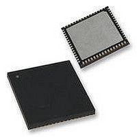
PIC18F65K90-I/MR Microchip Technology, PIC18F65K90-I/MR Datasheet - Page 286

PIC18F65K90-I/MR
Manufacturer Part Number
PIC18F65K90-I/MR
Description
32kB Flash, 2kB RAM, 1kB EE, NanoWatt XLP, LCD 64 QFN 9x9x0.9mm TUBE
Manufacturer
Microchip Technology
Series
PIC® XLP™ 18Fr
Datasheet
1.PIC18F65K90-IMR.pdf
(570 pages)
Specifications of PIC18F65K90-I/MR
Processor Series
PIC18F
Core
PIC
Data Bus Width
8 bit
Program Memory Type
Flash
Program Memory Size
32 KB
Data Ram Size
2 KB
Interface Type
I2C, SPI
Maximum Clock Frequency
64 MHz
Number Of Timers
8
Operating Supply Voltage
1.8 V to 5.5 V
Maximum Operating Temperature
+ 125 C
3rd Party Development Tools
52715-96, 52716-328, 52717-734, 52712-325, EWPIC18
Minimum Operating Temperature
- 40 C
On-chip Adc
12 bit, 16 Channel
Core Processor
PIC
Core Size
8-Bit
Speed
64MHz
Connectivity
I²C, LIN, SPI, UART/USART
Peripherals
Brown-out Detect/Reset, LCD, POR, PWM, WDT
Number Of I /o
53
Eeprom Size
1K x 8
Ram Size
2K x 8
Voltage - Supply (vcc/vdd)
1.8 V ~ 5.5 V
Data Converters
A/D 16x12b
Oscillator Type
Internal
Operating Temperature
-40°C ~ 85°C
Package / Case
64-VFQFN Exposed Pad
Lead Free Status / Rohs Status
Details
- Current page: 286 of 570
- Download datasheet (5Mb)
PIC18F87K90 FAMILY
20.7
The rate at which the COM and SEG outputs change is
called the LCD frame frequency.
TABLE 20-5:
TABLE 20-6:
DS39957D-page 286
Multiplex
LP<3:0>
Note:
Static
1/2
1/3
1/4
1
2
3
4
5
6
7
LCD Frame Frequency
Clock
Timer1 Osc/32 or INTRC/32.
Clock Source/(4 x 1 x (LP<3:0> + 1))
Clock Source/(2 x 2 x (LP<3:0> + 1))
Clock Source/(1 x 3 x (LP<3:0> + 1))
Clock Source/(1 x 4 x (LP<3:0> + 1))
Static
125
83
62
50
42
36
31
FRAME FREQUENCY
FORMULAS
APPROXIMATE FRAME
FREQUENCY (IN Hz) USING
F
32.768 kHz OR INTRC OSC
OSC
source
Frame Frequency =
AT 32 MHz, TIMER1 AT
125
1/2
83
62
50
42
36
31
is
167
111
1/3
83
67
56
48
42
(F
OSC
/4)/8192,
125
1/4
83
62
50
42
36
31
component and can take only one of the two rms values.
20.8
LCD waveform generation is based on the philosophy
that the net AC voltage across the dark pixel should be
maximized and the net AC voltage across the clear
pixel should be minimized. The net DC voltage across
any pixel should be zero.
The COM signal represents the time slice for each
common, while the SEG contains the pixel data.
The pixel signal (COM-SEG) will have no DC
The higher rms value will create a dark pixel and a lower
rms value will create a clear pixel.
As the number of commons increases, the delta
between the two rms values decreases. The delta
represents the maximum contrast that the display can
have.
The LCDs can be driven by two types of waveforms:
Type-A and Type-B. In a Type-A waveform, the phase
changes within each common type, whereas a Type-B
waveform’s phase changes on each frame boundary.
Thus, Type-A waveforms maintain 0 V
frame, whereas Type-B waveforms take two frames.
Figure 20-7
for static, half-multiplex, one-third multiplex and quarter
multiplex drives for Type-A and Type-B waveforms.
Note 1: If Sleep has to be executed with
2: When the LCD clock source is (F
LCD Waveform Generation
LCD
(LCDCON<6>) = 1), care must be taken
to execute Sleep only when V
the pixels is ‘0’.
8192, if Sleep is executed irrespective of
the LCDCON<SLPEN> setting, the LCD
goes into Sleep. Thus, take care to see
that V
executed.
through
DC
2009-2011 Microchip Technology Inc.
Sleep
Figure 20-17
on all pixels is ‘0’ when Sleep is
enabled
provide waveforms
DC
over a single
DC
(SLPEN
OSC
on all
/4)/
Related parts for PIC18F65K90-I/MR
Image
Part Number
Description
Manufacturer
Datasheet
Request
R

Part Number:
Description:
Manufacturer:
Microchip Technology Inc.
Datasheet:

Part Number:
Description:
Manufacturer:
Microchip Technology Inc.
Datasheet:

Part Number:
Description:
Manufacturer:
Microchip Technology Inc.
Datasheet:

Part Number:
Description:
Manufacturer:
Microchip Technology Inc.
Datasheet:

Part Number:
Description:
Manufacturer:
Microchip Technology Inc.
Datasheet:

Part Number:
Description:
Manufacturer:
Microchip Technology Inc.
Datasheet:

Part Number:
Description:
Manufacturer:
Microchip Technology Inc.
Datasheet:

Part Number:
Description:
Manufacturer:
Microchip Technology Inc.
Datasheet:


