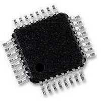
AT89C51CC02UA-RATUM Atmel, AT89C51CC02UA-RATUM Datasheet - Page 34

AT89C51CC02UA-RATUM
Manufacturer Part Number
AT89C51CC02UA-RATUM
Description
IC 8051 MCU 16K FLASH 32-VQFP
Manufacturer
Atmel
Series
AT89C CANr
Datasheet
1.T89C51CC02CA-TDSIM.pdf
(159 pages)
Specifications of AT89C51CC02UA-RATUM
Core Processor
8051
Core Size
8-Bit
Speed
40MHz
Connectivity
CAN, UART/USART
Peripherals
POR, PWM, WDT
Number Of I /o
20
Program Memory Size
16KB (16K x 8)
Program Memory Type
FLASH
Eeprom Size
2K x 8
Ram Size
512 x 8
Voltage - Supply (vcc/vdd)
3 V ~ 5.5 V
Data Converters
A/D 8x10b
Oscillator Type
External
Operating Temperature
-40°C ~ 85°C
Package / Case
32-TQFP, 32-VQFP
Processor Series
AT89x
Core
8051
Data Bus Width
8 bit
Data Ram Size
512 B
Interface Type
UART
Maximum Clock Frequency
40 MHz
Number Of Programmable I/os
20
Number Of Timers
1
Operating Supply Voltage
3 V to 5.5 V
Maximum Operating Temperature
+ 85 C
Mounting Style
SMD/SMT
3rd Party Development Tools
PK51, CA51, A51, ULINK2
Development Tools By Supplier
CANADAPT28
Minimum Operating Temperature
- 40 C
On-chip Adc
10 bit, 8 Channel
For Use With
AT89OCD-01 - USB EMULATOR FOR AT8XC51 MCU
Lead Free Status / RoHS Status
Lead free / RoHS Compliant
Available stocks
Company
Part Number
Manufacturer
Quantity
Price
Company:
Part Number:
AT89C51CC02UA-RATUM
Manufacturer:
Atmel
Quantity:
1 845
Program/Code
Memory
Flash Memory
Architecture
Figure 13. Flash Memory Architecture
34
AT/T89C51CC02
Hardware Security (1 byte)
Extra Row (128 Bytes)
Column Latches (128 Bytes)
The T89C51CC02 implement 16K Bytes of on-chip program/code memory.
The Flash memory increases EPROM and ROM functionality by in-circuit electrical era-
sure and programming. Thanks to the internal charge pump, the high voltage needed for
programming or erasing Flash cells is generated on-chip using the standard V
age. Thus, the Flash memory can be programmed using only one voltage and allows In-
System Programming (ISP). Hardware programming mode is also available using spe-
cific programming tool.
Figure 12. Program/Code Memory Organization
T89C51CC02 features two on-chip Flash memories:
•
•
The FM0 can be program by both parallel programming and Serial ISP whereas FM1
supports only parallel programming by programmers. The ISP mode is detailed in the
’In-System Programming’ section.
All Read/Write access operations on Flash memory by user application are managed by
a set of API described in the ’In-System Programming’ section.
3FFFh
0000h
Flash memory FM0:
containing 16K Bytes of program memory (user space) organized into 128 bytes
pages,
Flash memory FM1:
2K Bytes for boot loader and Application Programming Interfaces (API).
Flash Memory
16K Bytes
User Space
FM0
3FFFh
0000h
16K Bytes
Internal
Flash
FM1 mapped between F800h and
FFFFh when bit ENBOOT is set in
AUXR1 register
Flash Memory
Boot Space
2K Bytes
FM1
FFFFh
F800h
4126L–CAN–01/08
DD
volt-


