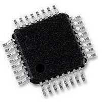
AT89C51CC02UA-RATUM Atmel, AT89C51CC02UA-RATUM Datasheet - Page 37

AT89C51CC02UA-RATUM
Manufacturer Part Number
AT89C51CC02UA-RATUM
Description
IC 8051 MCU 16K FLASH 32-VQFP
Manufacturer
Atmel
Series
AT89C CANr
Datasheet
1.T89C51CC02CA-TDSIM.pdf
(159 pages)
Specifications of AT89C51CC02UA-RATUM
Core Processor
8051
Core Size
8-Bit
Speed
40MHz
Connectivity
CAN, UART/USART
Peripherals
POR, PWM, WDT
Number Of I /o
20
Program Memory Size
16KB (16K x 8)
Program Memory Type
FLASH
Eeprom Size
2K x 8
Ram Size
512 x 8
Voltage - Supply (vcc/vdd)
3 V ~ 5.5 V
Data Converters
A/D 8x10b
Oscillator Type
External
Operating Temperature
-40°C ~ 85°C
Package / Case
32-TQFP, 32-VQFP
Processor Series
AT89x
Core
8051
Data Bus Width
8 bit
Data Ram Size
512 B
Interface Type
UART
Maximum Clock Frequency
40 MHz
Number Of Programmable I/os
20
Number Of Timers
1
Operating Supply Voltage
3 V to 5.5 V
Maximum Operating Temperature
+ 85 C
Mounting Style
SMD/SMT
3rd Party Development Tools
PK51, CA51, A51, ULINK2
Development Tools By Supplier
CANADAPT28
Minimum Operating Temperature
- 40 C
On-chip Adc
10 bit, 8 Channel
For Use With
AT89OCD-01 - USB EMULATOR FOR AT8XC51 MCU
Lead Free Status / RoHS Status
Lead free / RoHS Compliant
Available stocks
Company
Part Number
Manufacturer
Quantity
Price
Company:
Part Number:
AT89C51CC02UA-RATUM
Manufacturer:
Atmel
Quantity:
1 845
Status of the Flash Memory
Selecting FM1
Loading the Column Latches
4126L–CAN–01/08
The bit FBUSY in FCON register is used to indicate the status of programming.
FBUSY is set when programming is in progress.
The bit ENBOOT in AUXR1 register is used to map FM1 from F800h to FFFFh.
Any number of data from 1 byte to 128 Bytes can be loaded in the column latches. This
provides the capability to program the whole memory by byte, by page or by any number
of Bytes in a page.
When programming is launched, an automatic erase of the locations loaded in the col-
umn latches is first performed, then programming is effectively done. Thus no page or
block erase is needed and only the loaded data are programmed in the corresponding
page.
The following procedure is used to load the column latches and is summarized in
Figure 14:
•
•
•
•
•
•
Save then disable interrupt and map the column latch space by setting FPS bit.
Load the DPTR with the address to load.
Load Accumulator register with the data to load.
Execute the MOVX @DPTR, A instruction.
If needed loop the three last instructions until the page is completely loaded.
unmap the column latch and Restore Interrupt
AT/T89C51CC02
37


