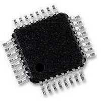
AT89C51CC02UA-RATUM Atmel, AT89C51CC02UA-RATUM Datasheet - Page 36

AT89C51CC02UA-RATUM
Manufacturer Part Number
AT89C51CC02UA-RATUM
Description
IC 8051 MCU 16K FLASH 32-VQFP
Manufacturer
Atmel
Series
AT89C CANr
Datasheet
1.T89C51CC02CA-TDSIM.pdf
(159 pages)
Specifications of AT89C51CC02UA-RATUM
Core Processor
8051
Core Size
8-Bit
Speed
40MHz
Connectivity
CAN, UART/USART
Peripherals
POR, PWM, WDT
Number Of I /o
20
Program Memory Size
16KB (16K x 8)
Program Memory Type
FLASH
Eeprom Size
2K x 8
Ram Size
512 x 8
Voltage - Supply (vcc/vdd)
3 V ~ 5.5 V
Data Converters
A/D 8x10b
Oscillator Type
External
Operating Temperature
-40°C ~ 85°C
Package / Case
32-TQFP, 32-VQFP
Processor Series
AT89x
Core
8051
Data Bus Width
8 bit
Data Ram Size
512 B
Interface Type
UART
Maximum Clock Frequency
40 MHz
Number Of Programmable I/os
20
Number Of Timers
1
Operating Supply Voltage
3 V to 5.5 V
Maximum Operating Temperature
+ 85 C
Mounting Style
SMD/SMT
3rd Party Development Tools
PK51, CA51, A51, ULINK2
Development Tools By Supplier
CANADAPT28
Minimum Operating Temperature
- 40 C
On-chip Adc
10 bit, 8 Channel
For Use With
AT89OCD-01 - USB EMULATOR FOR AT8XC51 MCU
Lead Free Status / RoHS Status
Lead free / RoHS Compliant
Available stocks
Company
Part Number
Manufacturer
Quantity
Price
Company:
Part Number:
AT89C51CC02UA-RATUM
Manufacturer:
Atmel
Quantity:
1 845
Overview of FM0
Operations
Mapping of the Memory Space By default, the user space is accessed by MOVC instruction for read only. The column
Launching Programming
36
AT/T89C51CC02
The CPU interfaces the Flash memory through the FCON register and AUXR1 register.
These registers are used to:
•
•
•
latches space is made accessible by setting the FPS bit in FCON register. Writing is
possible from 0000h to 3FFFh, address bits 6 to 0 are used to select an address within a
page while bits 14 to 7 are used to select the programming address of the page.
Setting FPS bit takes precedence on the EEE bit in EECON register.
The other memory spaces (user, extra row, hardware security) are made accessible in
the code segment by programming bits FMOD0 and FMOD1 in FCON register in accor-
dance with Table 22. A MOVC instruction is then used for reading these spaces.
Table 22. FM0 blocks Select bits
FPL3:0 bits in FCON register are used to secure the launch of programming. A specific
sequence must be written in these bits to unlock the write protection and to launch the
programming. This sequence is 5xh followed by Axh. Table 23 summarizes the memory
spaces to program according to FMOD1:0 bits.
Table 23. Programming Spaces
Note:
Extra Row
Hardware
Reserved
Security
User
Byte
Map the memory spaces in the adressable space
Launch the programming of the memory spaces
Get the status of the Flash memory (busy/not busy)
FMOD1
The sequence 5xh and Axh must be executing without instructions between them other-
wise the programming is aborted.
Interrupts that may occur during programming time must be disabled to avoid any spuri-
ous exit of the programming mode.
0
0
1
1
FPL3:0
A
A
A
A
5
5
5
5
FMOD0
FPS
0
1
0
1
Write to FCON
x
x
x
x
x
x
x
x
FMOD1
FM0 Adressable Space
User (0000h-3FFFh)
Extra Row(FF80h-FFFFh)
Hardware Security Byte (0000h)
Reserved
0
0
0
0
1
1
1
1
FMOD0
0
0
1
1
0
0
1
1
Operation
No action
Write the column latches in user
space
No action
Write the column latches in extra row
space
No action
Write the fuse bits space
No action
No action
4126L–CAN–01/08


