AT89C51CC02UA-RATUM Atmel, AT89C51CC02UA-RATUM Datasheet - Page 8
AT89C51CC02UA-RATUM
Manufacturer Part Number
AT89C51CC02UA-RATUM
Description
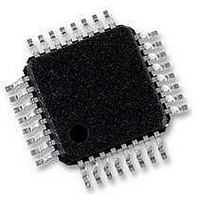
IC 8051 MCU 16K FLASH 32-VQFP
Manufacturer
Atmel
Series
AT89C CANr
Datasheet
1.T89C51CC02CA-TDSIM.pdf
(159 pages)
Specifications of AT89C51CC02UA-RATUM
Core Processor
8051
Core Size
8-Bit
Speed
40MHz
Connectivity
CAN, UART/USART
Peripherals
POR, PWM, WDT
Number Of I /o
20
Program Memory Size
16KB (16K x 8)
Program Memory Type
FLASH
Eeprom Size
2K x 8
Ram Size
512 x 8
Voltage - Supply (vcc/vdd)
3 V ~ 5.5 V
Data Converters
A/D 8x10b
Oscillator Type
External
Operating Temperature
-40°C ~ 85°C
Package / Case
32-TQFP, 32-VQFP
Processor Series
AT89x
Core
8051
Data Bus Width
8 bit
Data Ram Size
512 B
Interface Type
UART
Maximum Clock Frequency
40 MHz
Number Of Programmable I/os
20
Number Of Timers
1
Operating Supply Voltage
3 V to 5.5 V
Maximum Operating Temperature
+ 85 C
Mounting Style
SMD/SMT
3rd Party Development Tools
PK51, CA51, A51, ULINK2
Development Tools By Supplier
CANADAPT28
Minimum Operating Temperature
- 40 C
On-chip Adc
10 bit, 8 Channel
For Use With
AT89OCD-01 - USB EMULATOR FOR AT8XC51 MCU
Lead Free Status / RoHS Status
Lead free / RoHS Compliant
Available stocks
Company
Part Number
Manufacturer
Quantity
Price
Company:

Part Number:
AT89C51CC02UA-RATUM
Manufacturer:
Atmel
Quantity:
1 845


Read-Modify-Write
Instructions
Quasi Bi-directional Port
Operation
8
AT/T89C51CC02
Some instructions read the latch data rather than the pin data. The latch based instruc-
tions read the data, modify the data and then rewrite the latch. These are called ’Read-
Modify-Write’ instructions. Below is a complete list of these special instructions (See
Table 1). When the destination operand is a Port or a Port bit, these instructions read
the latch rather than the pin:
Table 1. Read/Modify/Write Instructions
It is not obvious that the last three instructions in this list are Read-Modify-Write instruc-
tions. These instructions read the port (all 8 bits), modify the specifically addressed bit
and write the new byte back to the latch. These Read-Modify-Write instructions are
directed to the latch rather than the pin in order to avoid possible misinterpretation of
voltage (and therefore, logic) levels at the pin. For example, a Port bit used to drive the
base of an external bipolar transistor cannot rise above the transistor’s base-emitter
junction voltage (a value lower than VIL). With a logic one written to the bit, attempts by
the CPU to read the Port at the pin are misinterpreted as logic zero. A read of the latch
rather than the pins returns the correct logic one value.
Port 1, Port 3 and Port 4 have fixed internal pull-ups and are referred to as ’quasi-bidi-
rectional’ Ports. When configured as an input, the pin impedance appears as logic one
and sources current in response to an external logic zero condition. Resets write logic
one to all Port latches. If logical zero is subsequently written to a Port latch, it can be
returned to input conditions by a logic one written to the latch.
Note:
Logical zero-to-one transitions in Port 1, Port 3 and Port 4 use an additional pull-up (p1)
to aid this logic transition See Figure 2. This increases switch speed. This extra pull-up
sources 100 times normal internal circuit current during 2 oscillator clock periods. The
internal pull-ups are field-effect transistors rather than linear resistors. Pull-ups consist
of three p-channel FET (pFET) devices. A pFET is on when the gate senses logic zero
and off when the gate senses logic one. pFET #1 is turned on for two oscillator periods
immediately after a zero-to-one transition in the Port latch. A logic one at the Port pin
turns on pFET #3 (a weak pull-up) through the inverter. This inverter and pFET pair form
a latch to drive logic one. pFET #2 is a very weak pull-up switched on whenever the
MOV Px.y, C
Instruction
CLR Px.y
SET Px.y
DJNZ
DEC
ANL
ORL
XRL
CPL
JBC
INC
Port latch values change near the end of Read-Modify-Write insruction cycles. Output
buffers (and therefore the pin state) are updated early in the instruction after Read-Mod-
ify-Write instruction cycle.
Description
Logical AND
Logical OR
Logical EX-OR
Jump if bit = 1 and clear bit
Complement bit
Increment
Decrement
Decrement and jump if not zero
Move carry bit to bit y of Port x
Clear bit y of Port x
Set bit y of Port x
Example
ANL P1, A
ORL P2, A
XRL P3, A
JBC P1.1, LABEL
CPL P3.0
INC P2
DEC P2
DJNZ P3, LABEL
MOV P1.5, C
CLR P2.4
SET P3.3
4126L–CAN–01/08
Related parts for AT89C51CC02UA-RATUM
Image
Part Number
Description
Manufacturer
Datasheet
Request
R

Part Number:
Description:
Manufacturer:
Atmel Corporation
Datasheet:
Part Number:
Description:
At89c51cc02, T89c51cc02 Enhanced 8-bit Microcontroller With Can Controller And Flash
Manufacturer:
ATMEL Corporation
Datasheet:

Part Number:
Description:
DEV KIT FOR AVR/AVR32
Manufacturer:
Atmel
Datasheet:
Part Number:
Description:
INTERVAL AND WIPE/WASH WIPER CONTROL IC WITH DELAY
Manufacturer:
ATMEL Corporation
Datasheet:
Part Number:
Description:
Low-Voltage Voice-Switched IC for Hands-Free Operation
Manufacturer:
ATMEL Corporation
Datasheet:
Part Number:
Description:
MONOLITHIC INTEGRATED FEATUREPHONE CIRCUIT
Manufacturer:
ATMEL Corporation
Datasheet:
Part Number:
Description:
AM-FM Receiver IC U4255BM-M
Manufacturer:
ATMEL Corporation
Datasheet:
Part Number:
Description:
Monolithic Integrated Feature Phone Circuit
Manufacturer:
ATMEL Corporation
Datasheet:
Part Number:
Description:
Multistandard Video-IF and Quasi Parallel Sound Processing
Manufacturer:
ATMEL Corporation
Datasheet:
Part Number:
Description:
High-performance EE PLD
Manufacturer:
ATMEL Corporation
Datasheet:
Part Number:
Description:
8-bit Flash Microcontroller
Manufacturer:
ATMEL Corporation
Datasheet:
Part Number:
Description:
2-Wire Serial EEPROM
Manufacturer:
ATMEL Corporation
Datasheet: