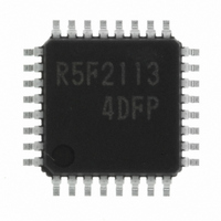
R5F21134DFP#U0 Renesas Electronics America, R5F21134DFP#U0 Datasheet - Page 187

R5F21134DFP#U0
Manufacturer Part Number
R5F21134DFP#U0
Description
IC R8C MCU FLASH 32LQFP
Manufacturer
Renesas Electronics America
Series
M16C™ M16C/R8C/Tiny/13r
Datasheets
1.R5F211A2SPU0.pdf
(300 pages)
2.R5F21132FPU0.pdf
(33 pages)
3.R5F21132FPU0.pdf
(226 pages)
4.R5F21134DFPU0.pdf
(224 pages)
Specifications of R5F21134DFP#U0
Core Size
16-Bit
Program Memory Size
16KB (16K x 8)
Oscillator Type
Internal
Core Processor
R8C
Speed
20MHz
Connectivity
SIO, UART/USART
Peripherals
LED, POR, Voltage Detect, WDT
Number Of I /o
22
Program Memory Type
FLASH
Ram Size
1K x 8
Voltage - Supply (vcc/vdd)
2.7 V ~ 5.5 V
Data Converters
A/D 12x10b
Operating Temperature
-40°C ~ 85°C
Package / Case
32-LQFP
No. Of I/o's
22
Eeprom Memory Size
4KB
Ram Memory Size
1024Byte
Cpu Speed
20MHz
No. Of Timers
16
Digital Ic Case
RoHS Compliant
Controller Family/series
R8C/13
Rohs Compliant
Yes
Lead Free Status / RoHS Status
Lead free / RoHS Compliant
For Use With
R0K521134S000BE - KIT EVAL STARTER FOR R8C/13R0E521134EPB00 - KIT EMULATOR PROBE FOR PC7501R0E521134CPE00 - EMULATOR COMPACT R8C/13
Eeprom Size
-
Lead Free Status / RoHS Status
Lead free / RoHS Compliant
Available stocks
Company
Part Number
Manufacturer
Quantity
Price
Part Number:
R5F21134DFP#U0R5F21134DFP
Manufacturer:
Renesas Electronics America
Quantity:
10 000
- R5F211A2SPU0 PDF datasheet
- R5F21132FPU0 PDF datasheet #2
- R5F21132FPU0 PDF datasheet #3
- R5F21134DFPU0 PDF datasheet #4
- Current page: 187 of 224
- Download datasheet (3Mb)
R8C/13 Group
Rev.1.20
REJ09B0111-0120
Figure 17.9 Program Command
• Program Command
Jan 27, 2006
This command writes data to the flash memory in one byte units.
Write ‘40
auto program operation (data program and verify) will start. Make sure the address value specified in
the first bus cycle is the same address as the write address specified in the second bus cycle.
Check the FMR00 bit in the FMR0 register to see if auto programming has finished. The FMR00 bit
is “0” during auto programming and set to “1” when auto programming is completed.
Check the FMR06 bit in the FMR0 register after auto programming has finished, and the result of
auto programming can be known. (Refer to Section 17.4.5, “Full Status Check.”)
Writing over already programmed addresses is inhibited.
When the FMR02 bit in the FMR0 register is set to “0” (rewrite disabled), or the FMR02 bit is set to “1”
(rewrite enabled) and the FMR15 bit in the FMR1 register is set to “1” (rewrite disabled), the program
command on the Block0 is not accepted. When the FMR16 bit is set to “1” (rewrite disabled), the
program command on the Block1 is not accepted.
In EW1 mode, do not execute this command on any address at which the rewrite control program is
located.
In EW0 mode, the microcomputer goes to read status register mode at the same time auto program-
ming starts, making it possible to read the status register. The status register bit 7 (SR7) is set to “0”
at the same time auto programming starts, and set back to “1” when auto programming finishes. In
this case, the microcomputer remains in read status register mode until a read array command is
written next. The result of auto programming can be known by reading the status register after auto
programming has finished.
16
’ in the first bus cycle and write data to the write address in the second bus cycle, and an
page 176 of 205
Write the command code ‘40
Write data to the write address
Full status check
the write address
FMR00=1?
completed
Program
Start
YES
NO
16
’ to
17.4 CPU Rewrite Mode
Related parts for R5F21134DFP#U0
Image
Part Number
Description
Manufacturer
Datasheet
Request
R

Part Number:
Description:
KIT STARTER FOR M16C/29
Manufacturer:
Renesas Electronics America
Datasheet:

Part Number:
Description:
KIT STARTER FOR R8C/2D
Manufacturer:
Renesas Electronics America
Datasheet:

Part Number:
Description:
R0K33062P STARTER KIT
Manufacturer:
Renesas Electronics America
Datasheet:

Part Number:
Description:
KIT STARTER FOR R8C/23 E8A
Manufacturer:
Renesas Electronics America
Datasheet:

Part Number:
Description:
KIT STARTER FOR R8C/25
Manufacturer:
Renesas Electronics America
Datasheet:

Part Number:
Description:
KIT STARTER H8S2456 SHARPE DSPLY
Manufacturer:
Renesas Electronics America
Datasheet:

Part Number:
Description:
KIT STARTER FOR R8C38C
Manufacturer:
Renesas Electronics America
Datasheet:

Part Number:
Description:
KIT STARTER FOR R8C35C
Manufacturer:
Renesas Electronics America
Datasheet:

Part Number:
Description:
KIT STARTER FOR R8CL3AC+LCD APPS
Manufacturer:
Renesas Electronics America
Datasheet:

Part Number:
Description:
KIT STARTER FOR RX610
Manufacturer:
Renesas Electronics America
Datasheet:

Part Number:
Description:
KIT STARTER FOR R32C/118
Manufacturer:
Renesas Electronics America
Datasheet:

Part Number:
Description:
KIT DEV RSK-R8C/26-29
Manufacturer:
Renesas Electronics America
Datasheet:

Part Number:
Description:
KIT STARTER FOR SH7124
Manufacturer:
Renesas Electronics America
Datasheet:

Part Number:
Description:
KIT STARTER FOR H8SX/1622
Manufacturer:
Renesas Electronics America
Datasheet:

Part Number:
Description:
KIT DEV FOR SH7203
Manufacturer:
Renesas Electronics America
Datasheet:


