R5F21134DFP#U0 Renesas Electronics America, R5F21134DFP#U0 Datasheet - Page 7
R5F21134DFP#U0
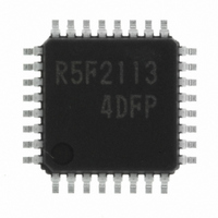
Manufacturer Part Number
R5F21134DFP#U0
Description
IC R8C MCU FLASH 32LQFP
Manufacturer
Renesas Electronics America
Series
M16C™ M16C/R8C/Tiny/13r
Datasheets
1.R5F211A2SPU0.pdf
(300 pages)
2.R5F21132FPU0.pdf
(33 pages)
3.R5F21132FPU0.pdf
(226 pages)
4.R5F21134DFPU0.pdf
(224 pages)
Specifications of R5F21134DFP#U0
Core Size
16-Bit
Program Memory Size
16KB (16K x 8)
Oscillator Type
Internal
Core Processor
R8C
Speed
20MHz
Connectivity
SIO, UART/USART
Peripherals
LED, POR, Voltage Detect, WDT
Number Of I /o
22
Program Memory Type
FLASH
Ram Size
1K x 8
Voltage - Supply (vcc/vdd)
2.7 V ~ 5.5 V
Data Converters
A/D 12x10b
Operating Temperature
-40°C ~ 85°C
Package / Case
32-LQFP
No. Of I/o's
22
Eeprom Memory Size
4KB
Ram Memory Size
1024Byte
Cpu Speed
20MHz
No. Of Timers
16
Digital Ic Case
RoHS Compliant
Controller Family/series
R8C/13
Rohs Compliant
Yes
Lead Free Status / RoHS Status
Lead free / RoHS Compliant
For Use With
R0K521134S000BE - KIT EVAL STARTER FOR R8C/13R0E521134EPB00 - KIT EMULATOR PROBE FOR PC7501R0E521134CPE00 - EMULATOR COMPACT R8C/13
Eeprom Size
-
Lead Free Status / RoHS Status
Lead free / RoHS Compliant
Available stocks
Company
Part Number
Manufacturer
Quantity
Price

Part Number:
R5F21134DFP#U0R5F21134DFP
Manufacturer:
Renesas Electronics America
Quantity:
10 000


Chapter 13. Serial Interface .............................................. 109
Chapter 14. A/D Converter................................................ 124
Chapter 15. Programmable I/O Ports .............................. 137
12.2 Timer Y......................................................................................................................... 80
12.3 Timer Z ......................................................................................................................... 88
12.4 Timer C ...................................................................................................................... 101
13.1 Clock Synchronous Serial I/O Mode ....................................................................... 114
13.2 Clock Asynchronous Serial I/O (UART) Mode ....................................................... 119
14.1 One-shot Mode ......................................................................................................... 128
14.2 Repeat Mode ............................................................................................................. 130
14.3 Sample and Hold ...................................................................................................... 132
14.4 A/D conversion cycles ........................................................................................... 132
14.5 Internal Equivalent Circuit of Analog Input ........................................................... 133
14.6 Inflow Current Bypass Circuit ................................................................................ 134
14.7 Output Impedance of Sensor under A/D Conversion........................................... 135
15.1 Description ................................................................................................................ 137
15.2 Port setting ................................................................................................................ 145
15.3 Unassigned Pin Handling ........................................................................................ 151
12.1.1 Timer Mode .......................................................................................................................................... 73
12.1.2 Pulse Output Mode ............................................................................................................................. 74
12.1.3 Event Counter Mode ........................................................................................................................... 75
12.1.4 Pulse Width Measurement Mode ....................................................................................................... 76
12.1.5 Pulse Period Measurement Mode ..................................................................................................... 78
12.2.1 Timer Mode .......................................................................................................................................... 83
12.2.2 Programmable Waveform Generation Mode .................................................................................... 85
12.3.1 Timer Mode .......................................................................................................................................... 91
12.3.2 Programmable Waveform Generation Mode .................................................................................... 93
12.3.3 Programmable One-shot Generation Mode ...................................................................................... 95
12.3.4 Programmable Wait One-shot Generation Mode ............................................................................. 98
12.4.1 Input Capture Mode ......................................................................................................................... 105
12.4.2 Output Compare Mode .................................................................................................................... 107
13.1.1 Polarity Select Function ................................................................................................................... 117
13.1.2 LSB First/MSB First Select Function .............................................................................................. 117
13.1.3 Continuous Receive Mode ............................................................................................................... 118
13.2.1 TxD10/RxD1 Select Function (UART1) ............................................................................................ 122
13.2.2 TxD11 Select Function (UART1) ...................................................................................................... 122
13.2.3 Bit Rate .............................................................................................................................................. 123
15.1.1 Port PiDirection Register (PDi Register, i=0,1,3,4) ......................................................................... 137
15.1.2 Port Pi Register (Pi Register, i=0 to 4) ............................................................................................. 137
15.1.3 Pull-up Control Register 0, Pull-up Control Register 1 (PUR0 and PUR1 registers) .................. 137
15.1.4 Port P1 Drive Capacity Control Register (DRR Register) .............................................................. 137
A-3
Related parts for R5F21134DFP#U0
Image
Part Number
Description
Manufacturer
Datasheet
Request
R

Part Number:
Description:
KIT STARTER FOR M16C/29
Manufacturer:
Renesas Electronics America
Datasheet:

Part Number:
Description:
KIT STARTER FOR R8C/2D
Manufacturer:
Renesas Electronics America
Datasheet:

Part Number:
Description:
R0K33062P STARTER KIT
Manufacturer:
Renesas Electronics America
Datasheet:

Part Number:
Description:
KIT STARTER FOR R8C/23 E8A
Manufacturer:
Renesas Electronics America
Datasheet:

Part Number:
Description:
KIT STARTER FOR R8C/25
Manufacturer:
Renesas Electronics America
Datasheet:

Part Number:
Description:
KIT STARTER H8S2456 SHARPE DSPLY
Manufacturer:
Renesas Electronics America
Datasheet:

Part Number:
Description:
KIT STARTER FOR R8C38C
Manufacturer:
Renesas Electronics America
Datasheet:

Part Number:
Description:
KIT STARTER FOR R8C35C
Manufacturer:
Renesas Electronics America
Datasheet:

Part Number:
Description:
KIT STARTER FOR R8CL3AC+LCD APPS
Manufacturer:
Renesas Electronics America
Datasheet:
Part Number:
Description:
KIT STARTER FOR RX610
Manufacturer:
Renesas Electronics America
Datasheet:

Part Number:
Description:
KIT STARTER FOR R32C/118
Manufacturer:
Renesas Electronics America
Datasheet:

Part Number:
Description:
KIT DEV RSK-R8C/26-29
Manufacturer:
Renesas Electronics America
Datasheet:

Part Number:
Description:
KIT STARTER FOR SH7124
Manufacturer:
Renesas Electronics America
Datasheet:

Part Number:
Description:
KIT STARTER FOR H8SX/1622
Manufacturer:
Renesas Electronics America
Datasheet:

Part Number:
Description:
KIT DEV FOR SH7203
Manufacturer:
Renesas Electronics America
Datasheet: