R5F21134DFP#U0 Renesas Electronics America, R5F21134DFP#U0 Datasheet - Page 198
R5F21134DFP#U0
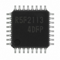
Manufacturer Part Number
R5F21134DFP#U0
Description
IC R8C MCU FLASH 32LQFP
Manufacturer
Renesas Electronics America
Series
M16C™ M16C/R8C/Tiny/13r
Datasheets
1.R5F211A2SPU0.pdf
(300 pages)
2.R5F21132FPU0.pdf
(33 pages)
3.R5F21132FPU0.pdf
(226 pages)
4.R5F21134DFPU0.pdf
(224 pages)
Specifications of R5F21134DFP#U0
Core Size
16-Bit
Program Memory Size
16KB (16K x 8)
Oscillator Type
Internal
Core Processor
R8C
Speed
20MHz
Connectivity
SIO, UART/USART
Peripherals
LED, POR, Voltage Detect, WDT
Number Of I /o
22
Program Memory Type
FLASH
Ram Size
1K x 8
Voltage - Supply (vcc/vdd)
2.7 V ~ 5.5 V
Data Converters
A/D 12x10b
Operating Temperature
-40°C ~ 85°C
Package / Case
32-LQFP
No. Of I/o's
22
Eeprom Memory Size
4KB
Ram Memory Size
1024Byte
Cpu Speed
20MHz
No. Of Timers
16
Digital Ic Case
RoHS Compliant
Controller Family/series
R8C/13
Rohs Compliant
Yes
Lead Free Status / RoHS Status
Lead free / RoHS Compliant
For Use With
R0K521134S000BE - KIT EVAL STARTER FOR R8C/13R0E521134EPB00 - KIT EMULATOR PROBE FOR PC7501R0E521134CPE00 - EMULATOR COMPACT R8C/13
Eeprom Size
-
Lead Free Status / RoHS Status
Lead free / RoHS Compliant
Available stocks
Company
Part Number
Manufacturer
Quantity
Price

Part Number:
R5F21134DFP#U0R5F21134DFP
Manufacturer:
Renesas Electronics America
Quantity:
10 000


R8C/13 Group
Rev.1.20
REJ09B0111-0120
19. Usage Notes
19.1 Stop Mode and Wait Mode
19.1.1 Stop Mode
19.1.2 Wait Mode
When entering stop mode, set the CM10 bit to “1” (stop mode) after setting the FMR01 bit to “0” (CPU
rewrite mode disabled). The instruction queue pre-reads 4 bytes from the instruction which sets the
CM10 bit in the CM1 register to “1” (stop mode) and the program stops. Insert at least 4 NOP instruc-
tions after inserting the JMP.B instruction immediately after the instruction which sets the CM10 bit to
“1”.
Use the next program to enter stop mode.
• Program of entering stop mode
When entering wait mode, execute the WAIT instruction after setting the FMR01 bit to “0” (CPU re-
write mode disabled). The instruction queue pre-reads 4 bytes from the WAIT instruction and the
program stops. Insert at least 4 NOP instructions after the WAIT instruction.
Also, the value in the specific internal RAM area may be rewritten when exiting wait mode if writing to
the interna RAM area before executing the WAIT instruction and entering wait mode. The area for a
maximum of 3 bytes is rewirtten from the following address of the internal RAM in which the writing is
performed before the WAIT instruction. If this causes a problem, avoid by inserting the JMP.B instruc-
tion between the writing instruction to the internal RAM area and WAIT instruction as shown in the
following program example.
• Example to execute WAIT instruction
When accessing any area other than the internal RAM area between the writing instruction to the
internal RAM area and execution of the WAIT instruction, this situation will not occur.
Jan 27, 2006
Program Example
page 187 of 205
LABEL_001 :
LABEL_001:
BCLR
BSET
BSET
JMP.B
NOP
NOP
NOP
NOP
MOV.B
•••
JMP.B
FSET
BCLR
WAIT
NOP
NOP
NOP
NOP
1, FMR0
0, PRCR
0, CM1
LABEL_001
#055h,0601h
LABEL_001
I
1,FMR0
; CPU rewrite mode disabled
; Protect exited
; Stop mode
; Write to internal RAM area
; Interrupt enabled
; CPU rewrite mode disabled
; Wait mode
19. Usage Notes
Related parts for R5F21134DFP#U0
Image
Part Number
Description
Manufacturer
Datasheet
Request
R

Part Number:
Description:
KIT STARTER FOR M16C/29
Manufacturer:
Renesas Electronics America
Datasheet:

Part Number:
Description:
KIT STARTER FOR R8C/2D
Manufacturer:
Renesas Electronics America
Datasheet:

Part Number:
Description:
R0K33062P STARTER KIT
Manufacturer:
Renesas Electronics America
Datasheet:

Part Number:
Description:
KIT STARTER FOR R8C/23 E8A
Manufacturer:
Renesas Electronics America
Datasheet:

Part Number:
Description:
KIT STARTER FOR R8C/25
Manufacturer:
Renesas Electronics America
Datasheet:

Part Number:
Description:
KIT STARTER H8S2456 SHARPE DSPLY
Manufacturer:
Renesas Electronics America
Datasheet:

Part Number:
Description:
KIT STARTER FOR R8C38C
Manufacturer:
Renesas Electronics America
Datasheet:

Part Number:
Description:
KIT STARTER FOR R8C35C
Manufacturer:
Renesas Electronics America
Datasheet:

Part Number:
Description:
KIT STARTER FOR R8CL3AC+LCD APPS
Manufacturer:
Renesas Electronics America
Datasheet:
Part Number:
Description:
KIT STARTER FOR RX610
Manufacturer:
Renesas Electronics America
Datasheet:

Part Number:
Description:
KIT STARTER FOR R32C/118
Manufacturer:
Renesas Electronics America
Datasheet:

Part Number:
Description:
KIT DEV RSK-R8C/26-29
Manufacturer:
Renesas Electronics America
Datasheet:

Part Number:
Description:
KIT STARTER FOR SH7124
Manufacturer:
Renesas Electronics America
Datasheet:

Part Number:
Description:
KIT STARTER FOR H8SX/1622
Manufacturer:
Renesas Electronics America
Datasheet:

Part Number:
Description:
KIT DEV FOR SH7203
Manufacturer:
Renesas Electronics America
Datasheet: