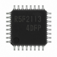
R5F21134DFP#U0 Renesas Electronics America, R5F21134DFP#U0 Datasheet - Page 37

R5F21134DFP#U0
Manufacturer Part Number
R5F21134DFP#U0
Description
IC R8C MCU FLASH 32LQFP
Manufacturer
Renesas Electronics America
Series
M16C™ M16C/R8C/Tiny/13r
Datasheets
1.R5F211A2SPU0.pdf
(300 pages)
2.R5F21132FPU0.pdf
(33 pages)
3.R5F21132FPU0.pdf
(226 pages)
4.R5F21134DFPU0.pdf
(224 pages)
Specifications of R5F21134DFP#U0
Core Size
16-Bit
Program Memory Size
16KB (16K x 8)
Oscillator Type
Internal
Core Processor
R8C
Speed
20MHz
Connectivity
SIO, UART/USART
Peripherals
LED, POR, Voltage Detect, WDT
Number Of I /o
22
Program Memory Type
FLASH
Ram Size
1K x 8
Voltage - Supply (vcc/vdd)
2.7 V ~ 5.5 V
Data Converters
A/D 12x10b
Operating Temperature
-40°C ~ 85°C
Package / Case
32-LQFP
No. Of I/o's
22
Eeprom Memory Size
4KB
Ram Memory Size
1024Byte
Cpu Speed
20MHz
No. Of Timers
16
Digital Ic Case
RoHS Compliant
Controller Family/series
R8C/13
Rohs Compliant
Yes
Lead Free Status / RoHS Status
Lead free / RoHS Compliant
For Use With
R0K521134S000BE - KIT EVAL STARTER FOR R8C/13R0E521134EPB00 - KIT EMULATOR PROBE FOR PC7501R0E521134CPE00 - EMULATOR COMPACT R8C/13
Eeprom Size
-
Lead Free Status / RoHS Status
Lead free / RoHS Compliant
Available stocks
Company
Part Number
Manufacturer
Quantity
Price
Part Number:
R5F21134DFP#U0R5F21134DFP
Manufacturer:
Renesas Electronics America
Quantity:
10 000
- R5F211A2SPU0 PDF datasheet
- R5F21132FPU0 PDF datasheet #2
- R5F21132FPU0 PDF datasheet #3
- R5F21134DFPU0 PDF datasheet #4
- Current page: 37 of 224
- Download datasheet (3Mb)
R8C/13 Group
Rev.1.20
REJ09B0111-0120
Table 5.2 Voltage Detection Interrupt Request Generation Conditions
NOTES:
N o r m a l o p e r a t i o n
m o d e
O p e r a t i o n m o d e
W a i t m o d e
1. The status except the wait mode and stop mode is handled as the normal mode. (Refer to Chapter 6, "Clock
2. Refer to Figure 5.14, "Operation Example of Voltage Detection Interrupt Generation Circuit" for interrupt generation
5.4.1 Voltage Detection Interrupt
Generation Circuit.")
timing.
Figure 5.13 shows the block diagram of voltage detection interrupt generation circuit.
Refer to 5.4.2, "Exiting Stop Mode on a Voltage Detection Circuit" for Getting out of stop mode due to
the voltage detection interrupt.
A voltage detection interrupt is generated when the input voltage at the V
or drops below Vdet if all of the following conditions hold true in normal operation mode and wait
mode.
To use the digital filter (D41 bit in the D4INT register is set to “0”), set the CM14 bit in the CM1 register
to "0" (low-speed on-chip oscillator on). Figure 5.14 shows an operation example of voltage detection
interrupt generation circuit.
The voltage detection interrupt shares the interrupt vector with the watchdog timer interrupt and oscil-
lation stop detection interrupt.
The D42 bit in the D4INT register becomes “1” when passing through Vdet is detected after the volt-
age inputted to the V
A voltage detection interrupt request is generated when the D42 bit changes state from “0” to “1”. The
D42 bit needs to be set to “0” in a program.
Table 5.2 lists the voltage detection interrupt request generation conditions.
It takes 4 cycles of sampling clock until the D42 bit is set to "1" since the voltage which inputs to
Vcc pin passes Vdet.
It is possible to set the sampling clock detecting that the voltage applied to the V
through Vdet with the DF0 to DF1 bits in the D4INT register.
(1 )
Jan 27, 2006
• The VC27 bit in the VCR2 register is set to “1” (voltage detection circuit enabled)
• The D40 bit in the D4INT register is set to “1” (voltage detection interrupt enabled)
• The D46 bit in the D4INT register is set “0” (voltage detection interrupt selected)
V C 2 7 b i t
1
1
page 26 of 205
CC
D40 bit
1
1
pin is up or down.
D 4 1 b i t
0 or 1
0 o r 1
D42 bit
0
0
D 4 6 b i t
0
0
F r o m 0 t o 1
F r o m 1 t o 0
F r o m 0 t o 1
F r o m 1 t o 0
VC13 bit
(2 )
(2 )
(2 )
(2 )
CC
CM14 bit
5.4 Voltage Detection Circuit
pin rises to Vdet or more
0
0
CC
pin has passed
Related parts for R5F21134DFP#U0
Image
Part Number
Description
Manufacturer
Datasheet
Request
R

Part Number:
Description:
KIT STARTER FOR M16C/29
Manufacturer:
Renesas Electronics America
Datasheet:

Part Number:
Description:
KIT STARTER FOR R8C/2D
Manufacturer:
Renesas Electronics America
Datasheet:

Part Number:
Description:
R0K33062P STARTER KIT
Manufacturer:
Renesas Electronics America
Datasheet:

Part Number:
Description:
KIT STARTER FOR R8C/23 E8A
Manufacturer:
Renesas Electronics America
Datasheet:

Part Number:
Description:
KIT STARTER FOR R8C/25
Manufacturer:
Renesas Electronics America
Datasheet:

Part Number:
Description:
KIT STARTER H8S2456 SHARPE DSPLY
Manufacturer:
Renesas Electronics America
Datasheet:

Part Number:
Description:
KIT STARTER FOR R8C38C
Manufacturer:
Renesas Electronics America
Datasheet:

Part Number:
Description:
KIT STARTER FOR R8C35C
Manufacturer:
Renesas Electronics America
Datasheet:

Part Number:
Description:
KIT STARTER FOR R8CL3AC+LCD APPS
Manufacturer:
Renesas Electronics America
Datasheet:

Part Number:
Description:
KIT STARTER FOR RX610
Manufacturer:
Renesas Electronics America
Datasheet:

Part Number:
Description:
KIT STARTER FOR R32C/118
Manufacturer:
Renesas Electronics America
Datasheet:

Part Number:
Description:
KIT DEV RSK-R8C/26-29
Manufacturer:
Renesas Electronics America
Datasheet:

Part Number:
Description:
KIT STARTER FOR SH7124
Manufacturer:
Renesas Electronics America
Datasheet:

Part Number:
Description:
KIT STARTER FOR H8SX/1622
Manufacturer:
Renesas Electronics America
Datasheet:

Part Number:
Description:
KIT DEV FOR SH7203
Manufacturer:
Renesas Electronics America
Datasheet:


