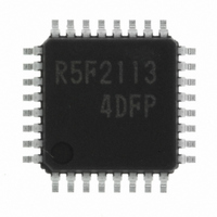
R5F21134DFP#U0 Renesas Electronics America, R5F21134DFP#U0 Datasheet - Page 191

R5F21134DFP#U0
Manufacturer Part Number
R5F21134DFP#U0
Description
IC R8C MCU FLASH 32LQFP
Manufacturer
Renesas Electronics America
Series
M16C™ M16C/R8C/Tiny/13r
Datasheets
1.R5F211A2SPU0.pdf
(300 pages)
2.R5F21132FPU0.pdf
(33 pages)
3.R5F21132FPU0.pdf
(226 pages)
4.R5F21134DFPU0.pdf
(224 pages)
Specifications of R5F21134DFP#U0
Core Size
16-Bit
Program Memory Size
16KB (16K x 8)
Oscillator Type
Internal
Core Processor
R8C
Speed
20MHz
Connectivity
SIO, UART/USART
Peripherals
LED, POR, Voltage Detect, WDT
Number Of I /o
22
Program Memory Type
FLASH
Ram Size
1K x 8
Voltage - Supply (vcc/vdd)
2.7 V ~ 5.5 V
Data Converters
A/D 12x10b
Operating Temperature
-40°C ~ 85°C
Package / Case
32-LQFP
No. Of I/o's
22
Eeprom Memory Size
4KB
Ram Memory Size
1024Byte
Cpu Speed
20MHz
No. Of Timers
16
Digital Ic Case
RoHS Compliant
Controller Family/series
R8C/13
Rohs Compliant
Yes
Lead Free Status / RoHS Status
Lead free / RoHS Compliant
For Use With
R0K521134S000BE - KIT EVAL STARTER FOR R8C/13R0E521134EPB00 - KIT EMULATOR PROBE FOR PC7501R0E521134CPE00 - EMULATOR COMPACT R8C/13
Eeprom Size
-
Lead Free Status / RoHS Status
Lead free / RoHS Compliant
Available stocks
Company
Part Number
Manufacturer
Quantity
Price
Part Number:
R5F21134DFP#U0R5F21134DFP
Manufacturer:
Renesas Electronics America
Quantity:
10 000
- R5F211A2SPU0 PDF datasheet
- R5F21132FPU0 PDF datasheet #2
- R5F21132FPU0 PDF datasheet #3
- R5F21134DFPU0 PDF datasheet #4
- Current page: 191 of 224
- Download datasheet (3Mb)
R8C/13 Group
Rev.1.20
REJ09B0111-0120
NOTES:
Table 17.6 Errors and FMR0 Register Status
1. Writing ‘FF
FMR07
(SR5)
mode, and the command code written in the first bus cycle is nullified.
(status register)
FRM00 register
17.4.5 Full Status Check
1
1
0
When an error occurs, the FMR06 to FMR07 bits in the FMR0 register are set to “1”, indicating occur-
rence of each specific error. Therefore, execution results can be verified by checking these status bits
(full status check). Table 17.6 lists errors and FMR0 register status. Figure 17.12 shows a full status
check flowchart and the action to be taken when each error occurs.
Jan 27, 2006
status
FMR06
(SR4)
16
1
’ in the second bus cycle of these commands places the microcomputer in read array
0
1
page 180 of 205
Command
sequence error • When invalid data was written other than those that can be writ-
Erase error
Program error
Error
• When any command is not written correctly
•When executing the program command or block erase command
• When inputting and erasing the address in which the Flash
• When executing to erase the block which disables rewriting dur-
• When inputting and writing the address in which the Flash
• When executing to write the block which disables rewriting during
• When the Block Erase command was executed but not automati-
• When the Program command was executed but not automatically
ten in the second bus cycle of the Block Erase command (i.e.,
other than ‘D0
while rewriting is disabled using the FMR02 bit in the FMR0 regis-
ter, the FMR15 or FMR16 bit in the FMR1 register.
memory is not allocated during the erase command input.
ing the erase command input.
memory is not allocated during the write command input.
the write command input.
cally erased correctly
programmed correctly.
16
’ or ‘FF
Error occurrence condition
16
’)
(1)
17.4 CPU Rewrite Mode
Related parts for R5F21134DFP#U0
Image
Part Number
Description
Manufacturer
Datasheet
Request
R

Part Number:
Description:
KIT STARTER FOR M16C/29
Manufacturer:
Renesas Electronics America
Datasheet:

Part Number:
Description:
KIT STARTER FOR R8C/2D
Manufacturer:
Renesas Electronics America
Datasheet:

Part Number:
Description:
R0K33062P STARTER KIT
Manufacturer:
Renesas Electronics America
Datasheet:

Part Number:
Description:
KIT STARTER FOR R8C/23 E8A
Manufacturer:
Renesas Electronics America
Datasheet:

Part Number:
Description:
KIT STARTER FOR R8C/25
Manufacturer:
Renesas Electronics America
Datasheet:

Part Number:
Description:
KIT STARTER H8S2456 SHARPE DSPLY
Manufacturer:
Renesas Electronics America
Datasheet:

Part Number:
Description:
KIT STARTER FOR R8C38C
Manufacturer:
Renesas Electronics America
Datasheet:

Part Number:
Description:
KIT STARTER FOR R8C35C
Manufacturer:
Renesas Electronics America
Datasheet:

Part Number:
Description:
KIT STARTER FOR R8CL3AC+LCD APPS
Manufacturer:
Renesas Electronics America
Datasheet:

Part Number:
Description:
KIT STARTER FOR RX610
Manufacturer:
Renesas Electronics America
Datasheet:

Part Number:
Description:
KIT STARTER FOR R32C/118
Manufacturer:
Renesas Electronics America
Datasheet:

Part Number:
Description:
KIT DEV RSK-R8C/26-29
Manufacturer:
Renesas Electronics America
Datasheet:

Part Number:
Description:
KIT STARTER FOR SH7124
Manufacturer:
Renesas Electronics America
Datasheet:

Part Number:
Description:
KIT STARTER FOR H8SX/1622
Manufacturer:
Renesas Electronics America
Datasheet:

Part Number:
Description:
KIT DEV FOR SH7203
Manufacturer:
Renesas Electronics America
Datasheet:


