R5F21134DFP#U0 Renesas Electronics America, R5F21134DFP#U0 Datasheet - Page 68
R5F21134DFP#U0
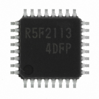
Manufacturer Part Number
R5F21134DFP#U0
Description
IC R8C MCU FLASH 32LQFP
Manufacturer
Renesas Electronics America
Series
M16C™ M16C/R8C/Tiny/13r
Datasheets
1.R5F211A2SPU0.pdf
(300 pages)
2.R5F21132FPU0.pdf
(33 pages)
3.R5F21132FPU0.pdf
(226 pages)
4.R5F21134DFPU0.pdf
(224 pages)
Specifications of R5F21134DFP#U0
Core Size
16-Bit
Program Memory Size
16KB (16K x 8)
Oscillator Type
Internal
Core Processor
R8C
Speed
20MHz
Connectivity
SIO, UART/USART
Peripherals
LED, POR, Voltage Detect, WDT
Number Of I /o
22
Program Memory Type
FLASH
Ram Size
1K x 8
Voltage - Supply (vcc/vdd)
2.7 V ~ 5.5 V
Data Converters
A/D 12x10b
Operating Temperature
-40°C ~ 85°C
Package / Case
32-LQFP
No. Of I/o's
22
Eeprom Memory Size
4KB
Ram Memory Size
1024Byte
Cpu Speed
20MHz
No. Of Timers
16
Digital Ic Case
RoHS Compliant
Controller Family/series
R8C/13
Rohs Compliant
Yes
Lead Free Status / RoHS Status
Lead free / RoHS Compliant
For Use With
R0K521134S000BE - KIT EVAL STARTER FOR R8C/13R0E521134EPB00 - KIT EMULATOR PROBE FOR PC7501R0E521134CPE00 - EMULATOR COMPACT R8C/13
Eeprom Size
-
Lead Free Status / RoHS Status
Lead free / RoHS Compliant
Available stocks
Company
Part Number
Manufacturer
Quantity
Price

Part Number:
R5F21134DFP#U0R5F21134DFP
Manufacturer:
Renesas Electronics America
Quantity:
10 000


R8C/13 Group
Rev.1.20
REJ09B0111-0120
Figure 10.6 Stack Status Before and After Acceptance of Interrupt Request
Figure 10.7 Operation of Saving Register
Address
• Saving Registers
m – 4
m – 3
m – 2
m – 1
m + 1
Stack status before interrupt request
is acknowledged
Jan 27, 2006
m
In the interrupt sequence, the FLG register and PC are saved to the stack.
At this time, the 4 high-order bits in the PC and the 4 high-order (IPL) and 8 low-order bits in the FLG
register, 16 bits in total, are saved to the stack first. Next, the 16 low-order bits in the PC are saved.
Figure 10.6 shows the stack status before and after an interrupt request is accepted.
The other necessary registers must be saved in a program at the beginning of the interrupt routine.
The PUSHM instruction can save several registers in the register bank being currently used
single instruction .
NOTES:
1. Selectable from registers R0, R1, R2, R3, A0, A1, SB, and FB.
The registers are saved in four steps, 8 bits at a time. Figure 10.7 shows the operation of the saving
registers.
NOTES:
1. When any INT instruction in software numbers 32 to 63 has been executed, this is the SP indi-
MSB
cated by the U flag. Otherwise, it is the ISP.
Content of previous stack
Content of previous stack
Stack
page 57 of 205
Address
[ S P ] – 5
[SP] – 4
[ S P ] – 3
[ S P ] – 2
[ S P ] – 1
[ S P ]
N O T E S :
1 . [ S P ] d e n o t e s t h e i n i t i a l v a l u e o f t h e S P w h e n i n t e r r u p t r e q u e s t i s a c k n o w l e d g e d .
A f t e r r e g i s t e r s a r e s a v e d , t h e S P c o n t e n t i s [ S P ] m i n u s 4 .
LSB
[SP]
SPvalue before
interrupt occurs
F L G
H
Stack
F L G
P C
P C
M
L
L
PC
H
Address
m – 4
m – 3
m – 2
m – 1
m
m + 1
Stack status after interrupt request
is acknowledged
MSB
S e q u e n c e i n w h i c h o r d e r
r e g i s t e r s a r e s a v e d
( 3 )
( 4 )
( 1 )
( 2 )
F i n i s h e d s a v i n g r e g i s t e r s
i n f o u r o p e r a t i o n s .
Content of previous stack
Content of previous stack
FLG
Saved, 8 bits at a time
H
Stack
PC
PC
FLG
L
M
L
PC
H
LSB
10.1 Interrupt Overview
[SP]
New SP value
(1)
with a
Related parts for R5F21134DFP#U0
Image
Part Number
Description
Manufacturer
Datasheet
Request
R

Part Number:
Description:
KIT STARTER FOR M16C/29
Manufacturer:
Renesas Electronics America
Datasheet:

Part Number:
Description:
KIT STARTER FOR R8C/2D
Manufacturer:
Renesas Electronics America
Datasheet:

Part Number:
Description:
R0K33062P STARTER KIT
Manufacturer:
Renesas Electronics America
Datasheet:

Part Number:
Description:
KIT STARTER FOR R8C/23 E8A
Manufacturer:
Renesas Electronics America
Datasheet:

Part Number:
Description:
KIT STARTER FOR R8C/25
Manufacturer:
Renesas Electronics America
Datasheet:

Part Number:
Description:
KIT STARTER H8S2456 SHARPE DSPLY
Manufacturer:
Renesas Electronics America
Datasheet:

Part Number:
Description:
KIT STARTER FOR R8C38C
Manufacturer:
Renesas Electronics America
Datasheet:

Part Number:
Description:
KIT STARTER FOR R8C35C
Manufacturer:
Renesas Electronics America
Datasheet:

Part Number:
Description:
KIT STARTER FOR R8CL3AC+LCD APPS
Manufacturer:
Renesas Electronics America
Datasheet:
Part Number:
Description:
KIT STARTER FOR RX610
Manufacturer:
Renesas Electronics America
Datasheet:

Part Number:
Description:
KIT STARTER FOR R32C/118
Manufacturer:
Renesas Electronics America
Datasheet:

Part Number:
Description:
KIT DEV RSK-R8C/26-29
Manufacturer:
Renesas Electronics America
Datasheet:

Part Number:
Description:
KIT STARTER FOR SH7124
Manufacturer:
Renesas Electronics America
Datasheet:

Part Number:
Description:
KIT STARTER FOR H8SX/1622
Manufacturer:
Renesas Electronics America
Datasheet:

Part Number:
Description:
KIT DEV FOR SH7203
Manufacturer:
Renesas Electronics America
Datasheet: