R5F21134DFP#U0 Renesas Electronics America, R5F21134DFP#U0 Datasheet - Page 190
R5F21134DFP#U0
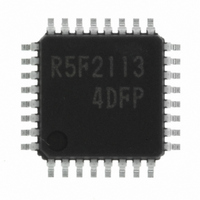
Manufacturer Part Number
R5F21134DFP#U0
Description
IC R8C MCU FLASH 32LQFP
Manufacturer
Renesas Electronics America
Series
M16C™ M16C/R8C/Tiny/13r
Datasheets
1.R5F211A2SPU0.pdf
(300 pages)
2.R5F21132FPU0.pdf
(33 pages)
3.R5F21132FPU0.pdf
(226 pages)
4.R5F21134DFPU0.pdf
(224 pages)
Specifications of R5F21134DFP#U0
Core Size
16-Bit
Program Memory Size
16KB (16K x 8)
Oscillator Type
Internal
Core Processor
R8C
Speed
20MHz
Connectivity
SIO, UART/USART
Peripherals
LED, POR, Voltage Detect, WDT
Number Of I /o
22
Program Memory Type
FLASH
Ram Size
1K x 8
Voltage - Supply (vcc/vdd)
2.7 V ~ 5.5 V
Data Converters
A/D 12x10b
Operating Temperature
-40°C ~ 85°C
Package / Case
32-LQFP
No. Of I/o's
22
Eeprom Memory Size
4KB
Ram Memory Size
1024Byte
Cpu Speed
20MHz
No. Of Timers
16
Digital Ic Case
RoHS Compliant
Controller Family/series
R8C/13
Rohs Compliant
Yes
Lead Free Status / RoHS Status
Lead free / RoHS Compliant
For Use With
R0K521134S000BE - KIT EVAL STARTER FOR R8C/13R0E521134EPB00 - KIT EMULATOR PROBE FOR PC7501R0E521134CPE00 - EMULATOR COMPACT R8C/13
Eeprom Size
-
Lead Free Status / RoHS Status
Lead free / RoHS Compliant
Available stocks
Company
Part Number
Manufacturer
Quantity
Price

Part Number:
R5F21134DFP#U0R5F21134DFP
Manufacturer:
Renesas Electronics America
Quantity:
10 000


R8C/13 Group
Rev.1.20
REJ09B0111-0120
Table 17.5 Status Register
• D
• The FMR07 bit (SR5) and FMR06 bit (SR4) are set to “0” by executing the Clear Status Register com-
• When the FMR07 bit (SR5) or FMR06 bit (SR4) = 1, the Program and Block Erase commands are not
mand.
accepted.
SR7 (D
SR6 (D
SR5 (D
SR4 (D
SR3 (D
SR2 (D
SR1 (D
SR0 (D
7
17.4.4 Status Register
register
Status
(1) When a given address in the user ROM area is read after writing the Read Status Register com-
(2) When a given address in the user ROM area is read after executing the Program or Block Erase
to D
The status register indicates the operating status of the flash memory and whether an erase or pro-
gramming operation terminated normally or in error. The status of the status register can be known by
reading the FMR00, FMR06, and FMR07 bits in the FMR0 register.
Table 17.5 lists the status register.
In EW0 mode, the status register can be read in the following cases:
• Sequence Status (SR7 and FMR00 Bits )
• Erase Status (SR5 and FMR07 Bits)
• Program Status (SR4 and FMR06 Bits)
Jan 27, 2006
The sequence status indicates the operating status of the flash memory. SR7 = 0 (busy) during auto
programming and auto erase, and is set to “1” (ready) at the same time the operation finishes.
Refer to Section 17.4.5, “Full Status Check.”
Refer to Section 17.4.5, “Full Status Check.”
bit
mand
command but before executing the Read Array command.
0
: Indicates the data bus which is read out when the Read Status Register command is executed.
7
6
5
4
3
2
1
0
)
)
)
)
)
)
)
)
register
FMR00
FMR07
FMR06
FMR0
bit
page 179 of 205
Program status
Reserved
Reserved
Reserved
Reserved
Reserved
Sequencer status
Erase status
Status name
Terminated normally
Terminated normally
Busy
"0"
-
-
-
-
-
Contents
Terminated in error
Terminated in error
Ready
"1"
-
-
-
-
-
17.4 CPU Rewrite Mode
Value
reset
after
1
0
0
Related parts for R5F21134DFP#U0
Image
Part Number
Description
Manufacturer
Datasheet
Request
R

Part Number:
Description:
KIT STARTER FOR M16C/29
Manufacturer:
Renesas Electronics America
Datasheet:

Part Number:
Description:
KIT STARTER FOR R8C/2D
Manufacturer:
Renesas Electronics America
Datasheet:

Part Number:
Description:
R0K33062P STARTER KIT
Manufacturer:
Renesas Electronics America
Datasheet:

Part Number:
Description:
KIT STARTER FOR R8C/23 E8A
Manufacturer:
Renesas Electronics America
Datasheet:

Part Number:
Description:
KIT STARTER FOR R8C/25
Manufacturer:
Renesas Electronics America
Datasheet:

Part Number:
Description:
KIT STARTER H8S2456 SHARPE DSPLY
Manufacturer:
Renesas Electronics America
Datasheet:

Part Number:
Description:
KIT STARTER FOR R8C38C
Manufacturer:
Renesas Electronics America
Datasheet:

Part Number:
Description:
KIT STARTER FOR R8C35C
Manufacturer:
Renesas Electronics America
Datasheet:

Part Number:
Description:
KIT STARTER FOR R8CL3AC+LCD APPS
Manufacturer:
Renesas Electronics America
Datasheet:
Part Number:
Description:
KIT STARTER FOR RX610
Manufacturer:
Renesas Electronics America
Datasheet:

Part Number:
Description:
KIT STARTER FOR R32C/118
Manufacturer:
Renesas Electronics America
Datasheet:

Part Number:
Description:
KIT DEV RSK-R8C/26-29
Manufacturer:
Renesas Electronics America
Datasheet:

Part Number:
Description:
KIT STARTER FOR SH7124
Manufacturer:
Renesas Electronics America
Datasheet:

Part Number:
Description:
KIT STARTER FOR H8SX/1622
Manufacturer:
Renesas Electronics America
Datasheet:

Part Number:
Description:
KIT DEV FOR SH7203
Manufacturer:
Renesas Electronics America
Datasheet: