R5F21134DFP#U0 Renesas Electronics America, R5F21134DFP#U0 Datasheet - Page 20
R5F21134DFP#U0
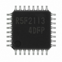
Manufacturer Part Number
R5F21134DFP#U0
Description
IC R8C MCU FLASH 32LQFP
Manufacturer
Renesas Electronics America
Series
M16C™ M16C/R8C/Tiny/13r
Datasheets
1.R5F211A2SPU0.pdf
(300 pages)
2.R5F21132FPU0.pdf
(33 pages)
3.R5F21132FPU0.pdf
(226 pages)
4.R5F21134DFPU0.pdf
(224 pages)
Specifications of R5F21134DFP#U0
Core Size
16-Bit
Program Memory Size
16KB (16K x 8)
Oscillator Type
Internal
Core Processor
R8C
Speed
20MHz
Connectivity
SIO, UART/USART
Peripherals
LED, POR, Voltage Detect, WDT
Number Of I /o
22
Program Memory Type
FLASH
Ram Size
1K x 8
Voltage - Supply (vcc/vdd)
2.7 V ~ 5.5 V
Data Converters
A/D 12x10b
Operating Temperature
-40°C ~ 85°C
Package / Case
32-LQFP
No. Of I/o's
22
Eeprom Memory Size
4KB
Ram Memory Size
1024Byte
Cpu Speed
20MHz
No. Of Timers
16
Digital Ic Case
RoHS Compliant
Controller Family/series
R8C/13
Rohs Compliant
Yes
Lead Free Status / RoHS Status
Lead free / RoHS Compliant
For Use With
R0K521134S000BE - KIT EVAL STARTER FOR R8C/13R0E521134EPB00 - KIT EMULATOR PROBE FOR PC7501R0E521134CPE00 - EMULATOR COMPACT R8C/13
Eeprom Size
-
Lead Free Status / RoHS Status
Lead free / RoHS Compliant
Available stocks
Company
Part Number
Manufacturer
Quantity
Price

Part Number:
R5F21134DFP#U0R5F21134DFP
Manufacturer:
Renesas Electronics America
Quantity:
10 000


R8C/13 Group
3. Memory
Rev.1.20
REJ09B0111-0120
Figure 3.1 Memory Map
Figure 3.1 is a memory map of this MCU. This MCU provides 1-Mbyte address space from addresses
00000
The internal ROM (program ROM) is allocated lower addresses beginning with address 0FFFF
example, a 16-Kbyte internal ROM is allocated addresses from 0C000
The fixed interrupt vector table is allocated addresses 0FFDC
address of each interrupt routine.
The internal ROM (data flash) is allocated addresses from 02000
The internal RAM is allocated higher addresses beginning with address 00400
internal RAM is allocated addresses 00400
data, but for calling subroutines and stacks when interrupt request is acknowledged.
Special function registers (SFR) are allocated addresses 00000
control registers are located them. All addresses, which have nothing allocated within the SFR, are re-
served area and cannot be accessed by users.
16
Jan 27, 2006
R5F21134FP, R5F21134DFP
R5F21133FP, R5F21133DFP
R5F21132FP, R5F21132DFP
to FFFFF
NOTES:
1. The data flash block A (2K bytes) and block B (2K bytes) are shown.
2. Blank spaces are reserved. No access is allowed.
0XXXX
0YYYY
FFFFF
0FFFF
00000
002FF
02FFF
00400
02000
Type name
16
16
16
16
16
16
16
16
16
16
(See Chapter 4 for details.)
.
page 9 of 205
(program ROM)
Expansion area
Internal ROM
Internal RAM
(data flash)
Internal ROM
SFR
(1)
16K bytes
12K bytes
8K bytes
Size
16
Internal ROM
to 007FF
Address 0YYYY
0FFFF
0FFDC
0C000
0D000
0E000
16
16
16
. The internal RAM is used not only for storing
16
16
16
Watchdog timer,Oscillation stop detection,Voltage detection
16
16
16
16
768 bytes
512 bytes
1K bytes
Size
to 02FFF
to 0FFFF
to 002FF
16
Internal RAM
Undefined instruction
to 0FFFF
BRK instruction
Address match
(Reserved)
Single step
(Reserved)
Overflow
Address 0XXXX
Reset
16
16
16
16
.
. They store the starting
. The peripheral function
007FF
006FF
005FF
. For example, a 1-Kbyte
16
.
16
16
16
16
16
3. Memory
. For
Related parts for R5F21134DFP#U0
Image
Part Number
Description
Manufacturer
Datasheet
Request
R

Part Number:
Description:
KIT STARTER FOR M16C/29
Manufacturer:
Renesas Electronics America
Datasheet:

Part Number:
Description:
KIT STARTER FOR R8C/2D
Manufacturer:
Renesas Electronics America
Datasheet:

Part Number:
Description:
R0K33062P STARTER KIT
Manufacturer:
Renesas Electronics America
Datasheet:

Part Number:
Description:
KIT STARTER FOR R8C/23 E8A
Manufacturer:
Renesas Electronics America
Datasheet:

Part Number:
Description:
KIT STARTER FOR R8C/25
Manufacturer:
Renesas Electronics America
Datasheet:

Part Number:
Description:
KIT STARTER H8S2456 SHARPE DSPLY
Manufacturer:
Renesas Electronics America
Datasheet:

Part Number:
Description:
KIT STARTER FOR R8C38C
Manufacturer:
Renesas Electronics America
Datasheet:

Part Number:
Description:
KIT STARTER FOR R8C35C
Manufacturer:
Renesas Electronics America
Datasheet:

Part Number:
Description:
KIT STARTER FOR R8CL3AC+LCD APPS
Manufacturer:
Renesas Electronics America
Datasheet:
Part Number:
Description:
KIT STARTER FOR RX610
Manufacturer:
Renesas Electronics America
Datasheet:

Part Number:
Description:
KIT STARTER FOR R32C/118
Manufacturer:
Renesas Electronics America
Datasheet:

Part Number:
Description:
KIT DEV RSK-R8C/26-29
Manufacturer:
Renesas Electronics America
Datasheet:

Part Number:
Description:
KIT STARTER FOR SH7124
Manufacturer:
Renesas Electronics America
Datasheet:

Part Number:
Description:
KIT STARTER FOR H8SX/1622
Manufacturer:
Renesas Electronics America
Datasheet:

Part Number:
Description:
KIT DEV FOR SH7203
Manufacturer:
Renesas Electronics America
Datasheet: