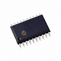
PIC16F785-I/SO Microchip Technology, PIC16F785-I/SO Datasheet - Page 116

PIC16F785-I/SO
Manufacturer Part Number
PIC16F785-I/SO
Description
IC PIC MCU FLASH 2KX14 20SOIC
Manufacturer
Microchip Technology
Series
PIC® 16Fr
Datasheets
1.PIC16F616T-ISL.pdf
(8 pages)
2.PIC16F785-ISS.pdf
(206 pages)
3.PIC16F785-ISS.pdf
(10 pages)
4.PIC16F785-ISS.pdf
(28 pages)
5.PIC16F785-IP.pdf
(178 pages)
Specifications of PIC16F785-I/SO
Program Memory Type
FLASH
Program Memory Size
3.5KB (2K x 14)
Package / Case
20-SOIC (7.5mm Width)
Core Processor
PIC
Core Size
8-Bit
Speed
20MHz
Peripherals
Brown-out Detect/Reset, POR, PWM, WDT
Number Of I /o
17
Eeprom Size
256 x 8
Ram Size
128 x 8
Voltage - Supply (vcc/vdd)
2 V ~ 5.5 V
Data Converters
A/D 14x10b
Oscillator Type
Internal
Operating Temperature
-40°C ~ 85°C
Processor Series
PIC16F
Core
PIC
Data Bus Width
8 bit
Data Ram Size
128 B
Interface Type
RS- 232/USB
Maximum Clock Frequency
20 MHz
Number Of Programmable I/os
17
Number Of Timers
3
Operating Supply Voltage
2 V to 5.5 V
Maximum Operating Temperature
+ 85 C
Mounting Style
SMD/SMT
3rd Party Development Tools
52715-96, 52716-328, 52717-734
Development Tools By Supplier
PG164130, DV164035, DV244005, DV164005, PG164120, ICE2000, DV164120, DM163029
Minimum Operating Temperature
- 40 C
On-chip Adc
14-ch x 10-bit
Lead Free Status / RoHS Status
Lead free / RoHS Compliant
For Use With
XLT20SO1-1 - SOCKET TRANS ICE 20DIP TO 20SOICXLT18SO-1 - SOCKET TRANSITION 18SOIC 300MILAC162060 - HEADER INTRFC MPLAB ICD2 20PINAC164039 - MODULE SKT PROMATE II 20DIP/SOIC
Connectivity
-
Lead Free Status / Rohs Status
Lead free / RoHS Compliant
Available stocks
Company
Part Number
Manufacturer
Quantity
Price
Part Number:
PIC16F785-I/SO
Manufacturer:
MICROCHIP/微芯
Quantity:
20 000
PIC16F785
15.4.1
External interrupt on RA2/AN2/T0CKI/INT/C1OUT pin
is edge-triggered; either rising, if INTEDG bit
(OPTION<6>) is set, or falling, if INTEDG bit is clear.
When a valid edge appears on the RA2/AN2/T0CKI/
INT/C1OUT pin, the INTF bit (INTCON<1>) is set. This
interrupt can be disabled by clearing the INTE control
bit (INTCON<4>). The INTF bit must be cleared in soft-
ware in the Interrupt Service Routine before re-
enabling this interrupt. The RA2/AN2/T0CKI/INT/
C1OUT interrupt can wake-up the processor from
Sleep if the INTE bit was set prior to going into Sleep.
The status of the GIE bit decides whether or not the
processor branches to the interrupt vector following
wake-up (0004h). See Section 15.7 “Power-Down
Mode (Sleep)” for details on Sleep and Figure 15-10
for timing of wake-up from Sleep through RA2/AN2/
T0CKI/INT/C1OUT interrupt.
FIGURE 15-7:
DS41249A-page 114
Note:
RA2/AN2/T0CKI/INT/C1OUT
INTERRUPT
The ANSEL0 (91h), and ANSEL1 (93h)
registers must be initialized to configure
an analog channel as a digital input. Pins
configured as analog inputs will read ‘0’.
IOC-RA0
IOC-RA1
IOC-RA2
IOC-RA3
IOC-RA4
IOC-RA5
TMR2IF
TMR2IE
TMR1IE
TMR1IF
CCP1IF
CCP1IE
IOCA0
IOCA1
IOCA2
IOCA3
IOCA4
IOCA5
OSFIF
OSFIE
ADIF
ADIE
EEIE
C1IF
C1IE
C2IF
C2IE
EEIF
INTERRUPT LOGIC
Preliminary
RAIE
INTF
INTE
RAIF
PEIE
T0IF
T0IE
GIE
15.4.2
An overflow (FFh
the T0IF (INTCON<2>) bit. The interrupt can be
enabled/disabled
(INTCON<5>) bit. See Section 5.0 “Timer0 Module”
for operation of the Timer0 module.
15.4.3
An input change on PORTA change sets the RAIF
(INTCON<0>) bit. The interrupt can be enabled/
disabled by setting/clearing the RAIE (INTCON<3>)
bit. Plus, individual pins can be configured through the
IOCA register.
Note:
TMR0 INTERRUPT
PORTA INTERRUPT
If a change on the I/O pin should occur
when the read operation is being executed
(start of the Q2 cycle), then the RAIF
interrupt flag may not get set.
Wake-up (If in Sleep mode)
00h) in the TMR0 register will set
by
2004 Microchip Technology Inc.
setting/clearing
Interrupt to CPU
T0IE


