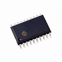
PIC16F785-I/SO Microchip Technology, PIC16F785-I/SO Datasheet - Page 81

PIC16F785-I/SO
Manufacturer Part Number
PIC16F785-I/SO
Description
IC PIC MCU FLASH 2KX14 20SOIC
Manufacturer
Microchip Technology
Series
PIC® 16Fr
Datasheets
1.PIC16F616T-ISL.pdf
(8 pages)
2.PIC16F785-ISS.pdf
(206 pages)
3.PIC16F785-ISS.pdf
(10 pages)
4.PIC16F785-ISS.pdf
(28 pages)
5.PIC16F785-IP.pdf
(178 pages)
Specifications of PIC16F785-I/SO
Program Memory Type
FLASH
Program Memory Size
3.5KB (2K x 14)
Package / Case
20-SOIC (7.5mm Width)
Core Processor
PIC
Core Size
8-Bit
Speed
20MHz
Peripherals
Brown-out Detect/Reset, POR, PWM, WDT
Number Of I /o
17
Eeprom Size
256 x 8
Ram Size
128 x 8
Voltage - Supply (vcc/vdd)
2 V ~ 5.5 V
Data Converters
A/D 14x10b
Oscillator Type
Internal
Operating Temperature
-40°C ~ 85°C
Processor Series
PIC16F
Core
PIC
Data Bus Width
8 bit
Data Ram Size
128 B
Interface Type
RS- 232/USB
Maximum Clock Frequency
20 MHz
Number Of Programmable I/os
17
Number Of Timers
3
Operating Supply Voltage
2 V to 5.5 V
Maximum Operating Temperature
+ 85 C
Mounting Style
SMD/SMT
3rd Party Development Tools
52715-96, 52716-328, 52717-734
Development Tools By Supplier
PG164130, DV164035, DV244005, DV164005, PG164120, ICE2000, DV164120, DM163029
Minimum Operating Temperature
- 40 C
On-chip Adc
14-ch x 10-bit
Lead Free Status / RoHS Status
Lead free / RoHS Compliant
For Use With
XLT20SO1-1 - SOCKET TRANS ICE 20DIP TO 20SOICXLT18SO-1 - SOCKET TRANSITION 18SOIC 300MILAC162060 - HEADER INTRFC MPLAB ICD2 20PINAC164039 - MODULE SKT PROMATE II 20DIP/SOIC
Connectivity
-
Lead Free Status / Rohs Status
Lead free / RoHS Compliant
Available stocks
Company
Part Number
Manufacturer
Quantity
Price
Part Number:
PIC16F785-I/SO
Manufacturer:
MICROCHIP/微芯
Quantity:
20 000
12.1.5
The A/D conversion is initiated by setting the
GO/DONE bit (ADCON0<1>). When the conversion is
complete, the A/D module:
• Clears the GO/DONE bit
• Sets the ADIF flag (PIR1<6>)
• Generates an interrupt (if enabled)
If the conversion must be aborted, the GO/DONE bit
can be cleared in software. The ADRESH:ADRESL
registers will not be updated with the partially complete
FIGURE 12-2:
12.1.6
The A/D conversion can be supplied in two formats: left
or right justified. The ADFM bit (ADCON0<7>) controls
the output format. Figure 12-3 shows the output
formats.
FIGURE 12-3:
2004 Microchip Technology Inc.
(ADFM = 0)
(ADFM = 1)
STARTING A CONVERSION
CONVERSION OUTPUT
T
CY
Set GO bit
Holding Capacitor is Disconnected from Analog Input (typically 100 ns)
to T
AD
Conversion Starts
A/D CONVERSION T
10-BIT A/D RESULT FORMAT
MSB
bit 7
bit 7
T
AD
Unimplemented: Read as ‘0’
1
T
AD
b9
2
T
AD
b8
ADRESH
3
T
10-bit A/D Result
AD
b7
AD
4
CYCLES
T
Preliminary
AD
b6
5
MSB
T
AD
b5
6
bit 0
bit 0
A/D
ADRESH:ADRESL registers will retain the value of the
previous conversion. After an aborted conversion, a
2 T
be initiated. Following the delay, an input acquisition is
automatically started on the selected channel.
ADRESH and ADRESL registers are loaded,
GO bit is cleared,
ADIF bit is set,
Holding capacitor is connected to analog input
T
AD
b4
Note:
AD
7
delay is required before another acquisition can
T
AD
b3
bit 7
bit 7
conversion
8
The GO/DONE bit should not be set in the
same instruction that turns on the A/D.
10-bit A/D Result
LSB
T
AD
b2
9
T
AD
b1
Unimplemented: Read as ‘0’
10 T
sample.
ADRESL
PIC16F785
AD
b0
11
DS41249A-page 79
Instead,
bit 0
LSB
bit 0
the


