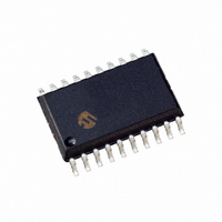
PIC16F785-I/SO Microchip Technology, PIC16F785-I/SO Datasheet - Page 63

PIC16F785-I/SO
Manufacturer Part Number
PIC16F785-I/SO
Description
IC PIC MCU FLASH 2KX14 20SOIC
Manufacturer
Microchip Technology
Series
PIC® 16Fr
Datasheets
1.PIC16F616T-ISL.pdf
(8 pages)
2.PIC16F785-ISS.pdf
(206 pages)
3.PIC16F785-ISS.pdf
(10 pages)
4.PIC16F785-ISS.pdf
(28 pages)
5.PIC16F785-IP.pdf
(178 pages)
Specifications of PIC16F785-I/SO
Program Memory Type
FLASH
Program Memory Size
3.5KB (2K x 14)
Package / Case
20-SOIC (7.5mm Width)
Core Processor
PIC
Core Size
8-Bit
Speed
20MHz
Peripherals
Brown-out Detect/Reset, POR, PWM, WDT
Number Of I /o
17
Eeprom Size
256 x 8
Ram Size
128 x 8
Voltage - Supply (vcc/vdd)
2 V ~ 5.5 V
Data Converters
A/D 14x10b
Oscillator Type
Internal
Operating Temperature
-40°C ~ 85°C
Processor Series
PIC16F
Core
PIC
Data Bus Width
8 bit
Data Ram Size
128 B
Interface Type
RS- 232/USB
Maximum Clock Frequency
20 MHz
Number Of Programmable I/os
17
Number Of Timers
3
Operating Supply Voltage
2 V to 5.5 V
Maximum Operating Temperature
+ 85 C
Mounting Style
SMD/SMT
3rd Party Development Tools
52715-96, 52716-328, 52717-734
Development Tools By Supplier
PG164130, DV164035, DV244005, DV164005, PG164120, ICE2000, DV164120, DM163029
Minimum Operating Temperature
- 40 C
On-chip Adc
14-ch x 10-bit
Lead Free Status / RoHS Status
Lead free / RoHS Compliant
For Use With
XLT20SO1-1 - SOCKET TRANS ICE 20DIP TO 20SOICXLT18SO-1 - SOCKET TRANSITION 18SOIC 300MILAC162060 - HEADER INTRFC MPLAB ICD2 20PINAC164039 - MODULE SKT PROMATE II 20DIP/SOIC
Connectivity
-
Lead Free Status / Rohs Status
Lead free / RoHS Compliant
Available stocks
Company
Part Number
Manufacturer
Quantity
Price
Part Number:
PIC16F785-I/SO
Manufacturer:
MICROCHIP/微芯
Quantity:
20 000
9.0
The comparator module has two separate voltage
comparators: Comparator C1 and Comparator C2.
Each comparator offers the following list of features:
• Control and configuration register
• Comparator output available externally
• Programmable output polarity
• Interrupt-on-change flags
• Wake-up from SLEEP
• Configurable as feedback input to the PWM
• Programmable four input multiplexer
• Programmable two input reference selections
• Programmable speed/power
• Output synchronization to Timer1 clock input
9.1
Both comparators have separate control and configura-
tion registers: CM1CON0 for C1 and CM2CON0 for C2.
In addition, Comparator C2 has a second control
register, CM2CON1, for synchronization control and
simultaneous reading of both comparator outputs.
9.1.1
The CM1CON0 register (shown in Register 9-1)
contains the control and Status bits for the following:
• Comparator enable
• Comparator input selection
• Comparator reference selection
• Output mode
• Comparator speed
Setting C1ON (CM1CON0<7>) enables Comparator
C1 for operation.
Bits C1CH<1:0> (CM1CON0<1:0>) select the compar-
ator input from the four analog pins AN<7:5,1>.
Setting C1R (CM1CON0<2>) selects the C1V
put of the comparator voltage reference module as the
reference voltage for the comparator. Clearing C1R
selects
RA0/AN0/C1IN+/ICSPDAT pin.
The output of the comparator is available internally via
the C1OUT flag (CM1CON0<6>). To make the output
available for an external connection, the C1OE bit
(CM1CON0<5>) must be set.
The polarity of the comparator output can be inverted
by setting the C1POL bit (CM1CON0<4>). Clearing
C1POL results in a non-inverted output.
2004 Microchip Technology Inc.
(Comparator C2 only)
Note:
COMPARATOR MODULE
Control Registers
To use AN<7:5,1> as analog inputs the
appropriate bits must be programmed to ‘1’
in the ANSEL0 register.
COMPARATOR C1 CONTROL
REGISTER
the
C1IN+
input
on
REF
out-
Preliminary
the
A complete table showing the output state versus input
conditions and the polarity bit is shown in Table 9-1.
TABLE 9-1:
C1SP (CM1CON0<3>) configures the speed of the
comparator. When C1SP is set, the comparator oper-
ates at its normal speed. Clearing C1SP operates the
comparator in a slower, low-power mode.
Input Condition
Note 1: The internal output of the comparator is
C1VN > C1VP
C1VN < C1VP
C1VN > C1VP
C1VN < C1VP
2: The C1 interrupt will operate correctly
3: To
latched at the end of each instruction
cycle. External outputs are not latched.
with C1OE set or cleared.
RA2/AN2/T0CKI/INT/C1OUT:
(C1OE=1) & (C1ON=1) & (TRISA<2>=0).
C1OUTPUT STATE VERSUS
INPUT CONDITIONS
C1POL
output
PIC16F785
0
0
1
1
DS41249A-page 61
C1
C1OUT
0
1
1
0
on


