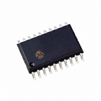
PIC16F785-I/SO Microchip Technology, PIC16F785-I/SO Datasheet - Page 75

PIC16F785-I/SO
Manufacturer Part Number
PIC16F785-I/SO
Description
IC PIC MCU FLASH 2KX14 20SOIC
Manufacturer
Microchip Technology
Series
PIC® 16Fr
Datasheets
1.PIC16F616T-ISL.pdf
(8 pages)
2.PIC16F785-ISS.pdf
(206 pages)
3.PIC16F785-ISS.pdf
(10 pages)
4.PIC16F785-ISS.pdf
(28 pages)
5.PIC16F785-IP.pdf
(178 pages)
Specifications of PIC16F785-I/SO
Program Memory Type
FLASH
Program Memory Size
3.5KB (2K x 14)
Package / Case
20-SOIC (7.5mm Width)
Core Processor
PIC
Core Size
8-Bit
Speed
20MHz
Peripherals
Brown-out Detect/Reset, POR, PWM, WDT
Number Of I /o
17
Eeprom Size
256 x 8
Ram Size
128 x 8
Voltage - Supply (vcc/vdd)
2 V ~ 5.5 V
Data Converters
A/D 14x10b
Oscillator Type
Internal
Operating Temperature
-40°C ~ 85°C
Processor Series
PIC16F
Core
PIC
Data Bus Width
8 bit
Data Ram Size
128 B
Interface Type
RS- 232/USB
Maximum Clock Frequency
20 MHz
Number Of Programmable I/os
17
Number Of Timers
3
Operating Supply Voltage
2 V to 5.5 V
Maximum Operating Temperature
+ 85 C
Mounting Style
SMD/SMT
3rd Party Development Tools
52715-96, 52716-328, 52717-734
Development Tools By Supplier
PG164130, DV164035, DV244005, DV164005, PG164120, ICE2000, DV164120, DM163029
Minimum Operating Temperature
- 40 C
On-chip Adc
14-ch x 10-bit
Lead Free Status / RoHS Status
Lead free / RoHS Compliant
For Use With
XLT20SO1-1 - SOCKET TRANS ICE 20DIP TO 20SOICXLT18SO-1 - SOCKET TRANSITION 18SOIC 300MILAC162060 - HEADER INTRFC MPLAB ICD2 20PINAC164039 - MODULE SKT PROMATE II 20DIP/SOIC
Connectivity
-
Lead Free Status / Rohs Status
Lead free / RoHS Compliant
Available stocks
Company
Part Number
Manufacturer
Quantity
Price
Part Number:
PIC16F785-I/SO
Manufacturer:
MICROCHIP/微芯
Quantity:
20 000
11.0
The OPA module has the following features:
• Two independent Operational Amplifiers
• External connections to all ports
• 3 MHz Gain Bandwidth Product (GBWP)
11.1
The OPA1CON register, shown in Register 11-1, controls
OPA1. OPA2CON, shown in Register 11-2, controls
OPA2.
FIGURE 11-1:
2004 Microchip Technology Inc.
OPERATIONAL AMPLIFIER
(OPA) MODULE
Control Registers
RC3/AN7/C12IN3-/OP1
RC2/AN6/C12IN2-/OP2
OPA MODULE BLOCK DIAGRAM
RB5/AN11/OP2+
RC7/AN9/OP1+
RB4/AN10/OP2-
RC6/AN8/OP1-
Preliminary
OPA1
OPA2
11.2
The OPA module is enabled by setting the OPAON bit
(OPAxCON<7>). When enabled, OPAON forces the
output driver of RC3/AN7/C12IN3-/OP1 for OPA1, and
RC2/AN6/C12IN2-/OP2 for OPA2, into tri-state to pre-
vent contention between the driver and the OPA output.
OPA1CON<OPAON>
OPA2CON<OPAON>
Note:
OPAxCON Register
TO ADC and Comparator MUXs
TO ADC and Comparator MUXs
When OPA1 or OPA2 is enabled, the
RC3/AN7/C12IN3-/OP1 pin, or
RC2/AN6/C12IN2-/OP2 pin respectively, is
driven by the op amp output, not by the
PORTC driver. Refer to the Electrical
specifications for the op amp output drive
capability.
PIC16F785
DS41249A-page 73


