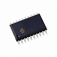
PIC16F785-I/SO Microchip Technology, PIC16F785-I/SO Datasheet - Page 89

PIC16F785-I/SO
Manufacturer Part Number
PIC16F785-I/SO
Description
IC PIC MCU FLASH 2KX14 20SOIC
Manufacturer
Microchip Technology
Series
PIC® 16Fr
Datasheets
1.PIC16F616T-ISL.pdf
(8 pages)
2.PIC16F785-ISS.pdf
(206 pages)
3.PIC16F785-ISS.pdf
(10 pages)
4.PIC16F785-ISS.pdf
(28 pages)
5.PIC16F785-IP.pdf
(178 pages)
Specifications of PIC16F785-I/SO
Program Memory Type
FLASH
Program Memory Size
3.5KB (2K x 14)
Package / Case
20-SOIC (7.5mm Width)
Core Processor
PIC
Core Size
8-Bit
Speed
20MHz
Peripherals
Brown-out Detect/Reset, POR, PWM, WDT
Number Of I /o
17
Eeprom Size
256 x 8
Ram Size
128 x 8
Voltage - Supply (vcc/vdd)
2 V ~ 5.5 V
Data Converters
A/D 14x10b
Oscillator Type
Internal
Operating Temperature
-40°C ~ 85°C
Processor Series
PIC16F
Core
PIC
Data Bus Width
8 bit
Data Ram Size
128 B
Interface Type
RS- 232/USB
Maximum Clock Frequency
20 MHz
Number Of Programmable I/os
17
Number Of Timers
3
Operating Supply Voltage
2 V to 5.5 V
Maximum Operating Temperature
+ 85 C
Mounting Style
SMD/SMT
3rd Party Development Tools
52715-96, 52716-328, 52717-734
Development Tools By Supplier
PG164130, DV164035, DV244005, DV164005, PG164120, ICE2000, DV164120, DM163029
Minimum Operating Temperature
- 40 C
On-chip Adc
14-ch x 10-bit
Lead Free Status / RoHS Status
Lead free / RoHS Compliant
For Use With
XLT20SO1-1 - SOCKET TRANS ICE 20DIP TO 20SOICXLT18SO-1 - SOCKET TRANSITION 18SOIC 300MILAC162060 - HEADER INTRFC MPLAB ICD2 20PINAC164039 - MODULE SKT PROMATE II 20DIP/SOIC
Connectivity
-
Lead Free Status / Rohs Status
Lead free / RoHS Compliant
Available stocks
Company
Part Number
Manufacturer
Quantity
Price
Part Number:
PIC16F785-I/SO
Manufacturer:
MICROCHIP/微芯
Quantity:
20 000
13.0
The two-phase PWM (Pulse Width Modulator) is a
stand-alone peripheral that supports:
• Single or dual-phase PWM
• Single complementary output PWM with overlap/
• Sync input/output to cascade devices for addi-
Setting either, or both, of the PH1EN or PH2EN bits of
the PWMCON0 register will activate the PWM module
(see Register 13-1). If PH1 is used then TRISC<1>
must be cleared to configure the pin as an output. The
same is true for TRISC<4> when using PH2.
13.1
The PWM period is derived from the main clock
(F
(see Figure 13-3). The prescale bits (PWMP<1:0>,
see Register 13-2) determine the value of the clock
divider which divides the system clock (F
pwm_clk. This pwm_clk is used to drive the PWM
counter. In Master mode, the PWM counter is reset
when the count reaches the period count (PER<4:0>,
see Register 13-2), which determines the frequency of
the PWM. The relationship between the PWM
frequency, prescale and period count is shown in
Equation 13-1.
EQUATION 13-1:
The maximum PWM frequency is F
period count must be greater than zero.
In Slave mode, the period counter is reset by the SYNC
input, which is the master device period counter reset.
For proper operation, the slave period count should be
equal to or greater than that of the master.
13.2
Each enabled phase output is driven active when the
phase counter matches the corresponding PWM phase
count (PH<4:0>, see Register 13-4 and Register 13-5).
The phase output remains true until terminated by a
feedback signal from either of the comparators or the
auto shutdown activates.
Phase granularity is a function of the period count
value. For example, if PER<4:0> = 3, each output can
be shifted in 90 steps (see Equation 13-2)
2004 Microchip Technology Inc.
delay
tional phases
OSC
PWM
), the PWM prescaler and the period counter
TWO-PHASE PWM
PWM Period
PWM Phase
FREQ
=
PWM FREQUENCY
--------------------------------------------------- -
2
PWMP
Fosc
PER
OSC
OSC
/2, since the
+
) to the
1
Preliminary
EQUATION 13-2:
13.3
Each PWM output is driven inactive, terminating the
drive period, by asynchronous feedback through the
internal comparators. The duty cycle resolution is in
effect infinitely adjustable. Either or both comparators
can be used to reset the PWM by setting the corre-
sponding comparator enable bit (CxEN, see
Register 13-3). Duty cycles of 100% can be obtained
by suppressing the feedback which would otherwise
terminate the pulse.
The comparator outputs can be “held off”, or blanked,
by enabling the corresponding BLANK bit (BLANKx,
see Register 13-1) for each phase. The blank bit
disables the comparator outputs for 1/2 of a system
clock (F
for the PWM output. Blanking avoids early termination
of the PWM output which may result due to switching
transients at the beginning of the cycle.
13.4
Multiple chips can operate together to achieve addi-
tional phases by operating one as the master and the
others as slaves. When the PWM is configured as a
master, the RB7/SYNC pin is an output and generates
a high output for one pwm_clk period at the end of
each PWM period (see Figure 13-4).
When the PWM is configured as a slave, the RB7/
SYNC pin is an input. The high input from a master in
this configuration resets the PWM period counter
which synchronizes the slave unit at the end of each
PWM period. Proper operation of a slave device
requires a common external F
drive the master and slave. The PWM prescale value
of the slave device must also be identical to that of the
master. As mentioned previously, the slave period
count value must be greater than or equal to that of
the master.
The PWM Counter will be reset and held at zero when
both PH1EN and PH2EN (PWMCON0<1:0>) are
false. If the PWM is configured as a slave, the PWM
Counter will remain reset at zero until the first SYNC
input is received.
OSC
PWM Duty Cycle
Master/Slave Operation
Phase
), thus ensuring at least Tosc/2 active time
DEG
PHASE RESOLUTION
=
PIC16F785
-------------------------
OSC
PER
360
clock source to
DS41249A-page 87
+
1


