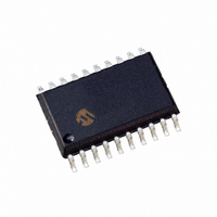
PIC16F785-I/SO Microchip Technology, PIC16F785-I/SO Datasheet - Page 96

PIC16F785-I/SO
Manufacturer Part Number
PIC16F785-I/SO
Description
IC PIC MCU FLASH 2KX14 20SOIC
Manufacturer
Microchip Technology
Series
PIC® 16Fr
Datasheets
1.PIC16F616T-ISL.pdf
(8 pages)
2.PIC16F785-ISS.pdf
(206 pages)
3.PIC16F785-ISS.pdf
(10 pages)
4.PIC16F785-ISS.pdf
(28 pages)
5.PIC16F785-IP.pdf
(178 pages)
Specifications of PIC16F785-I/SO
Program Memory Type
FLASH
Program Memory Size
3.5KB (2K x 14)
Package / Case
20-SOIC (7.5mm Width)
Core Processor
PIC
Core Size
8-Bit
Speed
20MHz
Peripherals
Brown-out Detect/Reset, POR, PWM, WDT
Number Of I /o
17
Eeprom Size
256 x 8
Ram Size
128 x 8
Voltage - Supply (vcc/vdd)
2 V ~ 5.5 V
Data Converters
A/D 14x10b
Oscillator Type
Internal
Operating Temperature
-40°C ~ 85°C
Processor Series
PIC16F
Core
PIC
Data Bus Width
8 bit
Data Ram Size
128 B
Interface Type
RS- 232/USB
Maximum Clock Frequency
20 MHz
Number Of Programmable I/os
17
Number Of Timers
3
Operating Supply Voltage
2 V to 5.5 V
Maximum Operating Temperature
+ 85 C
Mounting Style
SMD/SMT
3rd Party Development Tools
52715-96, 52716-328, 52717-734
Development Tools By Supplier
PG164130, DV164035, DV244005, DV164005, PG164120, ICE2000, DV164120, DM163029
Minimum Operating Temperature
- 40 C
On-chip Adc
14-ch x 10-bit
Lead Free Status / RoHS Status
Lead free / RoHS Compliant
For Use With
XLT20SO1-1 - SOCKET TRANS ICE 20DIP TO 20SOICXLT18SO-1 - SOCKET TRANSITION 18SOIC 300MILAC162060 - HEADER INTRFC MPLAB ICD2 20PINAC164039 - MODULE SKT PROMATE II 20DIP/SOIC
Connectivity
-
Lead Free Status / Rohs Status
Lead free / RoHS Compliant
Available stocks
Company
Part Number
Manufacturer
Quantity
Price
Part Number:
PIC16F785-I/SO
Manufacturer:
MICROCHIP/微芯
Quantity:
20 000
PIC16F785
13.7
Figure 13-7 shows an example of a single phase buck
voltage regulator application. The PWM output drives
Q1 with pulses to alternately charge and discharge L1.
C4 holds the charge from L1 during the inactive cycle
of the drive period. R4 and C3 form a ramp generator.
At the beginning of the PWM period, the PWM output
goes high causing the voltage on C3 to rise concur-
rently with the current in L1. When the voltage across
C3 reaches the threshold level present at the positive
input of comparator 1, the comparator output changes
and terminates the drive output from the PWM to Q1.
When Q1 is not driven, the current path to L1 through
Q1 is interrupted, but since the current in L1 cannot
stop instantly, the current continues to flow through D2
as L1 discharges into C4. D1 quickly discharges C3 in
preparation of the next ramp cycle.
FIGURE 13-7: EXAMPLE SINGLE PHASE APPLICATION
DS41249A-page 94
R1
C1
C2
Example single phase application
R2
R3
C5
OPA1
CCP
VR
C1
PIC16F785
Preliminary
2 PHASE
PWM
F
OSC
Resistor divider R5 and R6 scale the output voltage,
which is inverted and amplified by Op Amp 1 relative to
the reference voltage present at the non-inverting pin of
the op amp. R3, C5 and C2 form the inverting stabiliza-
tion gain feedback of the amplifier. The VR reference
supplies a stable reference to the non-inverting input of
the op amp, which is tweaked by the voltage source
created by a secondary time based PWM output of the
CCP and R1 and C1.
Output regulation occurs by the following principle: If
the regulator output voltage is too low, then the voltage
to the non-inverting input of comparator 1 will rise,
resulting in a higher threshold voltage and conse-
quently longer PWM drive pulses into Q1. If the output
voltage is too high, then the voltage to the non-inverting
input of comparator 1 will fall, resulting in shorter PWM
drive pulses into Q1.
PH1
R4
FET
DRIVER
C3
D1
2004 Microchip Technology Inc.
V
Q1
UNREG
D2
L1
C4
R5
R6


