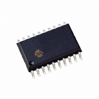
PIC16F785-I/SO Microchip Technology, PIC16F785-I/SO Datasheet - Page 38

PIC16F785-I/SO
Manufacturer Part Number
PIC16F785-I/SO
Description
IC PIC MCU FLASH 2KX14 20SOIC
Manufacturer
Microchip Technology
Series
PIC® 16Fr
Datasheets
1.PIC16F616T-ISL.pdf
(8 pages)
2.PIC16F785-ISS.pdf
(206 pages)
3.PIC16F785-ISS.pdf
(10 pages)
4.PIC16F785-ISS.pdf
(28 pages)
5.PIC16F785-IP.pdf
(178 pages)
Specifications of PIC16F785-I/SO
Program Memory Type
FLASH
Program Memory Size
3.5KB (2K x 14)
Package / Case
20-SOIC (7.5mm Width)
Core Processor
PIC
Core Size
8-Bit
Speed
20MHz
Peripherals
Brown-out Detect/Reset, POR, PWM, WDT
Number Of I /o
17
Eeprom Size
256 x 8
Ram Size
128 x 8
Voltage - Supply (vcc/vdd)
2 V ~ 5.5 V
Data Converters
A/D 14x10b
Oscillator Type
Internal
Operating Temperature
-40°C ~ 85°C
Processor Series
PIC16F
Core
PIC
Data Bus Width
8 bit
Data Ram Size
128 B
Interface Type
RS- 232/USB
Maximum Clock Frequency
20 MHz
Number Of Programmable I/os
17
Number Of Timers
3
Operating Supply Voltage
2 V to 5.5 V
Maximum Operating Temperature
+ 85 C
Mounting Style
SMD/SMT
3rd Party Development Tools
52715-96, 52716-328, 52717-734
Development Tools By Supplier
PG164130, DV164035, DV244005, DV164005, PG164120, ICE2000, DV164120, DM163029
Minimum Operating Temperature
- 40 C
On-chip Adc
14-ch x 10-bit
Lead Free Status / RoHS Status
Lead free / RoHS Compliant
For Use With
XLT20SO1-1 - SOCKET TRANS ICE 20DIP TO 20SOICXLT18SO-1 - SOCKET TRANSITION 18SOIC 300MILAC162060 - HEADER INTRFC MPLAB ICD2 20PINAC164039 - MODULE SKT PROMATE II 20DIP/SOIC
Connectivity
-
Lead Free Status / Rohs Status
Lead free / RoHS Compliant
Available stocks
Company
Part Number
Manufacturer
Quantity
Price
Part Number:
PIC16F785-I/SO
Manufacturer:
MICROCHIP/微芯
Quantity:
20 000
PIC16F785
4.2.3
Each PORTA pin is multiplexed with other functions.
The pins and their combined functions are briefly
described here. For specific information about individ-
ual functions such as the comparator or the A/D, refer
to the appropriate section in this Data Sheet.
4.2.3.1
Figure 4-1 shows the diagram for this pin. The RA0 pin
is configurable to function as one of the following:
• a general purpose I/O
• an analog input for the A/D
• an analog input to comparator 1
• In-Circuit Serial Programming
FIGURE 4-1:
DS41249A-page 36
DATA BUS
INTERRUPT-ON-
PORTA
PORTA
WPUA
WPUA
TRISA
TRISA
IOCA
IOCA
WR
WR
WR
WR
RD
RD
RD
RD
CHANGE
TO COMPARATOR
TO A/D CONVERTER
D
D
D
D
PORTA PIN DESCRIPTIONS AND
DIAGRAMS
CK
CK
CK
CK
RA0/AN0/C1IN+/ICSPDAT
Q
Q
Q
Q
Q
Q
Q
Q
BLOCK DIAGRAM OF RA0
RD PORTA
ANS0
RAPU
ANS0
™
Q
Q
Q
data
EN
EN
EN
D
D
D
V
DD
WEAK
Q1
V
V
DD
SS
I/O PIN
Q3
Preliminary
4.2.3.2
Figure 4-1 shows the diagram for this pin. The RA1 pin
is configurable to function as one of the following:
• a general purpose I/O
• an analog input for the A/D
• an analog input to comparators 1 & 2
• a voltage reference input for the A/D
• a buffered or unbuffered voltage reference output
• In-Circuit Serial Programming clock
FIGURE 4-2:
DATA BUS
INTERRUPT-ON-
VR
VROE*VREN
CVROE
ANS1
PORTA
PORTA
WPUA
WPUA
TRISA
TRISA
IOCA
IOCA
WR
WR
WR
WR
RD
RD
RD
RD
OUT
CHANGE
D
D
D
D
CK
TO COMPARATORS
TO A/D CONVERTER
CK
CK
CK
RA1/AN1/C12IN0-/V
Q
Q
Q
Q
Q
Q
Q
Q
BLOCK DIAGRAM OF RA1
RD PORTA
2004 Microchip Technology Inc.
RAPU
Q
Q
Q
EN
EN
EN
REF
D
D
D
/ICSPCLK
V
DD
Q1
V
V
WEAK
DD
SS
I/O PIN
Q3


