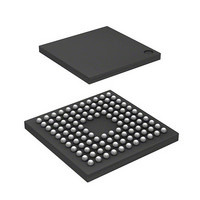
DF2214BQ16V Renesas Electronics America, DF2214BQ16V Datasheet - Page 14

DF2214BQ16V
Manufacturer Part Number
DF2214BQ16V
Description
IC H8S/2214 MCU FLASH 112-TFBGA
Manufacturer
Renesas Electronics America
Series
H8® H8S/2200r
Datasheets
1.HS2214ECB62H.pdf
(938 pages)
2.HEWH8E10A.pdf
(19 pages)
3.D12312SVTE25V.pdf
(341 pages)
Specifications of DF2214BQ16V
Core Processor
H8S/2000
Core Size
16-Bit
Speed
16MHz
Connectivity
SCI
Peripherals
DMA, POR, PWM, WDT
Number Of I /o
72
Program Memory Size
128KB (128K x 8)
Program Memory Type
FLASH
Ram Size
12K x 8
Voltage - Supply (vcc/vdd)
2.7 V ~ 3.6 V
Data Converters
D/A 1x8b
Oscillator Type
Internal
Operating Temperature
-20°C ~ 75°C
Package / Case
112-TFBGA
For Use With
HS0005KCU11H - EMULATOR E10A-USB H8S(X),SH2(A)3DK2218 - DEV EVAL KIT H8S/2218
Lead Free Status / RoHS Status
Lead free / RoHS Compliant
Eeprom Size
-
Available stocks
Company
Part Number
Manufacturer
Quantity
Price
Company:
Part Number:
DF2214BQ16V
Manufacturer:
Renesas Electronics America
Quantity:
10 000
- Current page: 14 of 938
- Download datasheet (6Mb)
Item
8.3.8 Chain
Transfer
8.5 Usage Notes
(1) Module Stop
9.2.2 Register
Configuration
(1) Port 1 Data
Direction Register
(P1DDR)
9.3.2 Register
Configuration
(1) Port 3 Data
Direction Register
(P3DDR)
9.5.2 Register
Configuration
(1) Port 7 Data
Direction Register
(P7DDR)
9.7.2 Register
Configuration
(1) Port A Data
Direction Register
(PADDR)
Rev.4.00 Sep. 18, 2008 Page xii of lx
REJ09B0189-0400
Page
273
280
286
297
309
316
Revisions (See Manual for Details)
Description added
Figure 8.9 shows the memory map for chain transfer. The DTC
reads the start address for the register information from the DTC
vector address corresponding to the DTC activation factor. After
the data transfer completes, the CHNE bit in this register is tested,
and if it is 1, the next register information allocated sequentially is
read and a transfer is performed. This operation continues until a
data transfer for register information whose CHNE bit is 0
completes.
Description added
... However, 1 cannot be written in the MSTPA6 bit while the DTC
is operating. See section 17, Power-Down Modes, for details.
Description added
... P1DDR cannot be read; if it is, an undefined value will be read.
Setting a P1DDR bit to 1 makes the corresponding port 1 pin an
output pin, while clearing the bit to 0, makes that pin an input pin.
Since this register is a write-only register, do not use bit
manipulation instructions to write to this register. See section
2.10.4, Access Methods for Registers with Write-Only Bits.
Description added
Setting a P3DDR bit to 1 makes the corresponding port 3 pin an
output pin, while clearing the bit to 0 makes the pin an input pin.
Since this register is a write-only register, do not use bit
manipulation instructions to write to this register. See section
2.10.4, Access Methods for Registers with Write-Only Bits.
Description added
Setting a P7DDR bit to 1 makes the corresponding port 7 pin an
output pin, while clearing the bit to 0 makes the pin an input pin.
Since this register is a write-only register, do not use bit
manipulation instructions to write to this register. See section
2.10.4, Access Methods for Registers with Write-Only Bits.
Description added
Bits 7 to 4 are reserved; these bits cannot be modified and will
return an undefined value if read. Since this register is a write-only
register, do not use bit manipulation instructions to write to this
register. See section 2.10.4, Access Methods for Registers with
Write-Only Bits.
Related parts for DF2214BQ16V
Image
Part Number
Description
Manufacturer
Datasheet
Request
R

Part Number:
Description:
CONN SOCKET 2POS 7.92MM WHITE
Manufacturer:
Hirose Electric Co Ltd
Datasheet:

Part Number:
Description:
CONN SOCKET 4POS 7.92MM WHITE
Manufacturer:
Hirose Electric Co Ltd
Datasheet:

Part Number:
Description:
CONN SOCKET 5POS 7.92MM WHITE
Manufacturer:
Hirose Electric Co Ltd
Datasheet:

Part Number:
Description:
CONN SOCKET 3POS 7.92MM WHITE
Manufacturer:
Hirose Electric Co Ltd
Datasheet:

Part Number:
Description:
CONN SOCKET 5POS 7.92MM WHITE
Manufacturer:
Hirose Electric Co Ltd
Datasheet:

Part Number:
Description:
CONN SOCKET 2POS 7.92MM WHITE
Manufacturer:
Hirose Electric Co Ltd
Datasheet:

Part Number:
Description:
CONN SOCKET 3POS 7.92MM WHITE
Manufacturer:
Hirose Electric Co Ltd
Datasheet:

Part Number:
Description:
CONN SOCKET 4POS 7.92MM WHITE
Manufacturer:
Hirose Electric Co Ltd
Datasheet:

Part Number:
Description:
CONN HEADER 2POS 7.92MM R/A TIN
Manufacturer:
Hirose Electric Co Ltd
Datasheet:

Part Number:
Description:
CONN HEADER 4POS 7.92MM R/A TIN
Manufacturer:
Hirose Electric Co Ltd
Datasheet:

Part Number:
Description:
KIT STARTER FOR M16C/29
Manufacturer:
Renesas Electronics America
Datasheet:

Part Number:
Description:
KIT STARTER FOR R8C/2D
Manufacturer:
Renesas Electronics America
Datasheet:

Part Number:
Description:
R0K33062P STARTER KIT
Manufacturer:
Renesas Electronics America
Datasheet:

Part Number:
Description:
KIT STARTER FOR R8C/23 E8A
Manufacturer:
Renesas Electronics America
Datasheet:

Part Number:
Description:
KIT STARTER FOR R8C/25
Manufacturer:
Renesas Electronics America
Datasheet:


