DF2214BQ16V Renesas Electronics America, DF2214BQ16V Datasheet - Page 51
DF2214BQ16V
Manufacturer Part Number
DF2214BQ16V
Description
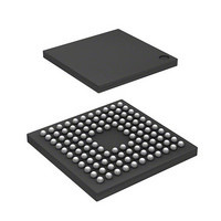
IC H8S/2214 MCU FLASH 112-TFBGA
Manufacturer
Renesas Electronics America
Series
H8® H8S/2200r
Datasheets
1.HS2214ECB62H.pdf
(938 pages)
2.HEWH8E10A.pdf
(19 pages)
3.D12312SVTE25V.pdf
(341 pages)
Specifications of DF2214BQ16V
Core Processor
H8S/2000
Core Size
16-Bit
Speed
16MHz
Connectivity
SCI
Peripherals
DMA, POR, PWM, WDT
Number Of I /o
72
Program Memory Size
128KB (128K x 8)
Program Memory Type
FLASH
Ram Size
12K x 8
Voltage - Supply (vcc/vdd)
2.7 V ~ 3.6 V
Data Converters
D/A 1x8b
Oscillator Type
Internal
Operating Temperature
-20°C ~ 75°C
Package / Case
112-TFBGA
For Use With
HS0005KCU11H - EMULATOR E10A-USB H8S(X),SH2(A)3DK2218 - DEV EVAL KIT H8S/2218
Lead Free Status / RoHS Status
Lead free / RoHS Compliant
Eeprom Size
-
Available stocks
Company
Part Number
Manufacturer
Quantity
Price
Company:

Part Number:
DF2214BQ16V
Manufacturer:
Renesas Electronics America
Quantity:
10 000


Figure 10.11 Example of Toggle Output Operation ..................................................................... 396
Figure 10.12 Example of Input Capture Operation Setting Procedure ......................................... 397
Figure 10.13 Example of Input Capture Operation....................................................................... 398
Figure 10.14 Example of Synchronous Operation Setting Procedure .......................................... 399
Figure 10.15 Example of Synchronous Operation........................................................................ 400
Figure 10.16 Compare Match Buffer Operation........................................................................... 401
Figure 10.17 Input Capture Buffer Operation............................................................................... 402
Figure 10.18 Example of Buffer Operation Setting Procedure..................................................... 402
Figure 10.19 Example of Buffer Operation (1) ............................................................................ 403
Figure 10.20 Example of Buffer Operation (2) ............................................................................ 404
Figure 10.21 Example of PWM Mode Setting Procedure ............................................................ 407
Figure 10.22 Example of PWM Mode Operation (1) ................................................................... 408
Figure 10.23 Example of PWM Mode Operation (2) ................................................................... 409
Figure 10.24 Example of PWM Mode Operation (3) ................................................................... 410
Figure 10.25 Example of Phase Counting Mode Setting Procedure............................................. 411
Figure 10.26 Example of Phase Counting Mode 1 Operation ...................................................... 412
Figure 10.27 Example of Phase Counting Mode 2 Operation ...................................................... 413
Figure 10.28 Example of Phase Counting Mode 3 Operation ...................................................... 414
Figure 10.29 Example of Phase Counting Mode 4 Operation ...................................................... 415
Figure 10.30 Count Timing in Internal Clock Operation.............................................................. 418
Figure 10.31 Count Timing in External Clock Operation ............................................................ 418
Figure 10.32 Output Compare Output Timing ............................................................................. 419
Figure 10.33 Input Capture Input Signal Timing.......................................................................... 420
Figure 10.34 Counter Clear Timing (Compare Match) ................................................................ 421
Figure 10.35 Counter Clear Timing (Input Capture) .................................................................... 421
Figure 10.36 Buffer Operation Timing (Compare Match) ........................................................... 422
Figure 10.37 Buffer Operation Timing (Input Capture) ............................................................... 422
Figure 10.38 TGI Interrupt Timing (Compare Match) ................................................................. 423
Figure 10.39 TGI Interrupt Timing (Input Capture) ..................................................................... 424
Figure 10.40 TCIV Interrupt Setting Timing................................................................................ 425
Figure 10.41 TCIU Interrupt Setting Timing................................................................................ 425
Figure 10.42 Timing for Status Flag Clearing by CPU ................................................................ 426
Figure 10.43 Timing for Status Flag Clearing by DTC/DMAC Activation ................................. 426
Figure 10.44 Phase Difference, Overlap, and Pulse Width in Phase Counting Mode .................. 427
Figure 10.45 Contention between TCNT Write and Clear Operations......................................... 428
Figure 10.46 Contention between TCNT Write and Increment Operations ................................. 429
Figure 10.47 Contention between TGR Write and Compare Match............................................. 430
Figure 10.48 Contention between Buffer Register Write and Compare Match............................ 431
Figure 10.49 Contention between TGR Read and Input Capture ................................................. 432
Figure 10.50 Contention between TGR Write and Input Capture ................................................ 433
Figure 10.51 Contention between Buffer Register Write and Input Capture................................ 434
Rev.4.00 Sep. 18, 2008 Page xlix of lx
REJ09B0189-0400
Related parts for DF2214BQ16V
Image
Part Number
Description
Manufacturer
Datasheet
Request
R

Part Number:
Description:
CONN SOCKET 2POS 7.92MM WHITE
Manufacturer:
Hirose Electric Co Ltd
Datasheet:

Part Number:
Description:
CONN SOCKET 4POS 7.92MM WHITE
Manufacturer:
Hirose Electric Co Ltd
Datasheet:

Part Number:
Description:
CONN SOCKET 5POS 7.92MM WHITE
Manufacturer:
Hirose Electric Co Ltd
Datasheet:

Part Number:
Description:
CONN SOCKET 3POS 7.92MM WHITE
Manufacturer:
Hirose Electric Co Ltd
Datasheet:
Part Number:
Description:
CONN SOCKET 5POS 7.92MM WHITE
Manufacturer:
Hirose Electric Co Ltd
Datasheet:

Part Number:
Description:
CONN SOCKET 2POS 7.92MM WHITE
Manufacturer:
Hirose Electric Co Ltd
Datasheet:
Part Number:
Description:
CONN SOCKET 3POS 7.92MM WHITE
Manufacturer:
Hirose Electric Co Ltd
Datasheet:
Part Number:
Description:
CONN SOCKET 4POS 7.92MM WHITE
Manufacturer:
Hirose Electric Co Ltd
Datasheet:

Part Number:
Description:
CONN HEADER 2POS 7.92MM R/A TIN
Manufacturer:
Hirose Electric Co Ltd
Datasheet:

Part Number:
Description:
CONN HEADER 4POS 7.92MM R/A TIN
Manufacturer:
Hirose Electric Co Ltd
Datasheet:

Part Number:
Description:
KIT STARTER FOR M16C/29
Manufacturer:
Renesas Electronics America
Datasheet:

Part Number:
Description:
KIT STARTER FOR R8C/2D
Manufacturer:
Renesas Electronics America
Datasheet:

Part Number:
Description:
R0K33062P STARTER KIT
Manufacturer:
Renesas Electronics America
Datasheet:

Part Number:
Description:
KIT STARTER FOR R8C/23 E8A
Manufacturer:
Renesas Electronics America
Datasheet:

Part Number:
Description:
KIT STARTER FOR R8C/25
Manufacturer:
Renesas Electronics America
Datasheet: