DF2214BQ16V Renesas Electronics America, DF2214BQ16V Datasheet - Page 60
DF2214BQ16V
Manufacturer Part Number
DF2214BQ16V
Description
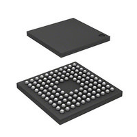
IC H8S/2214 MCU FLASH 112-TFBGA
Manufacturer
Renesas Electronics America
Series
H8® H8S/2200r
Datasheets
1.HS2214ECB62H.pdf
(938 pages)
2.HEWH8E10A.pdf
(19 pages)
3.D12312SVTE25V.pdf
(341 pages)
Specifications of DF2214BQ16V
Core Processor
H8S/2000
Core Size
16-Bit
Speed
16MHz
Connectivity
SCI
Peripherals
DMA, POR, PWM, WDT
Number Of I /o
72
Program Memory Size
128KB (128K x 8)
Program Memory Type
FLASH
Ram Size
12K x 8
Voltage - Supply (vcc/vdd)
2.7 V ~ 3.6 V
Data Converters
D/A 1x8b
Oscillator Type
Internal
Operating Temperature
-20°C ~ 75°C
Package / Case
112-TFBGA
For Use With
HS0005KCU11H - EMULATOR E10A-USB H8S(X),SH2(A)3DK2218 - DEV EVAL KIT H8S/2218
Lead Free Status / RoHS Status
Lead free / RoHS Compliant
Eeprom Size
-
Available stocks
Company
Part Number
Manufacturer
Quantity
Price
Company:

Part Number:
DF2214BQ16V
Manufacturer:
Renesas Electronics America
Quantity:
10 000


Table 10.12 Interrupt Sources and DMA Controller (DMAC) and Data Transfer (DTC)
Section 11 Watchdog Timer (WDT)
Table 11.1
Section 12 Serial Communication Interface (SCI)
Table 12.1
Table 12.2
Table 12.3
Table 12.4
Table 12.5
Table 12.6
Table 12.7
Table 12.8
Table 12.9
Table 12.10 SMR0, SCR0, SEMR0 Settings and SCI Clock Source Selection (SCI0 Only) ..... 489
Table 12.11 Serial Transfer Formats (Asynchronous Mode) ...................................................... 491
Table 12.12 Receive Errors and Conditions for Occurrence....................................................... 500
Table 12.13 SCI Interrupt Sources .............................................................................................. 519
Table 12.14 State of SSR Status Flags and Transfer of Receive Data ....................................... 521
Section 13 D/A Converter
Table 13.1
Table 13.2
Section 14 RAM
Table 14.1
Section 15 ROM
Table 15.1
Table 15.2
Table 15.3
Table 15.4
Table 15.5
Table 15.6
Table 15.7
Table 15.8
Table 15.9
Rev.4.00 Sep. 18, 2008 Page lviii of lx
REJ09B0189-0400
Activation................................................................................................................ 416
WDT Registers........................................................................................................ 439
SCI Pins................................................................................................................... 457
SCI Registers........................................................................................................... 458
BRR Settings for Various Bit Rates (Asynchronous Mode) ................................... 473
BRR Settings for Various Bit Rates (Clocked Synchronous Mode) ....................... 476
Maximum Bit Rate for Each Frequency (Asynchronous Mode, when ABCS = 0). 478
Maximum Bit Rate with External Clock Input
(Asynchronous Mode, when ABCS = 0)................................................................ 479
Maximum Bit Rate with External Clock Input (Clocked Synchronous Mode)....... 479
SMR Settings and Serial Transfer Format Selection............................................... 488
SMR and SCR Settings and SCI Clock Source Selection ....................................... 488
Pin Configuration .................................................................................................... 533
D/A Converter Registers ......................................................................................... 533
RAM Register ......................................................................................................... 540
ROM Register ......................................................................................................... 544
Operating Modes and ROM Area (F-ZTAT Version and Masked ROM Version) 545
Differences between Boot Mode and User Program Mode..................................... 552
Pin Configuration .................................................................................................... 554
Register Configuration ............................................................................................ 555
Flash Memory Erase Blocks.................................................................................... 561
Flash Memory Area Divisions ................................................................................ 562
Setting On-Board Programming Modes.................................................................. 564
System Clock Frequencies for which Automatic Adjustment of LSI Bit Rate Is
Possible ................................................................................................................... 567
Related parts for DF2214BQ16V
Image
Part Number
Description
Manufacturer
Datasheet
Request
R

Part Number:
Description:
CONN SOCKET 2POS 7.92MM WHITE
Manufacturer:
Hirose Electric Co Ltd
Datasheet:

Part Number:
Description:
CONN SOCKET 4POS 7.92MM WHITE
Manufacturer:
Hirose Electric Co Ltd
Datasheet:

Part Number:
Description:
CONN SOCKET 5POS 7.92MM WHITE
Manufacturer:
Hirose Electric Co Ltd
Datasheet:

Part Number:
Description:
CONN SOCKET 3POS 7.92MM WHITE
Manufacturer:
Hirose Electric Co Ltd
Datasheet:
Part Number:
Description:
CONN SOCKET 5POS 7.92MM WHITE
Manufacturer:
Hirose Electric Co Ltd
Datasheet:

Part Number:
Description:
CONN SOCKET 2POS 7.92MM WHITE
Manufacturer:
Hirose Electric Co Ltd
Datasheet:
Part Number:
Description:
CONN SOCKET 3POS 7.92MM WHITE
Manufacturer:
Hirose Electric Co Ltd
Datasheet:
Part Number:
Description:
CONN SOCKET 4POS 7.92MM WHITE
Manufacturer:
Hirose Electric Co Ltd
Datasheet:

Part Number:
Description:
CONN HEADER 2POS 7.92MM R/A TIN
Manufacturer:
Hirose Electric Co Ltd
Datasheet:

Part Number:
Description:
CONN HEADER 4POS 7.92MM R/A TIN
Manufacturer:
Hirose Electric Co Ltd
Datasheet:

Part Number:
Description:
KIT STARTER FOR M16C/29
Manufacturer:
Renesas Electronics America
Datasheet:

Part Number:
Description:
KIT STARTER FOR R8C/2D
Manufacturer:
Renesas Electronics America
Datasheet:

Part Number:
Description:
R0K33062P STARTER KIT
Manufacturer:
Renesas Electronics America
Datasheet:

Part Number:
Description:
KIT STARTER FOR R8C/23 E8A
Manufacturer:
Renesas Electronics America
Datasheet:

Part Number:
Description:
KIT STARTER FOR R8C/25
Manufacturer:
Renesas Electronics America
Datasheet: