DF2214BQ16V Renesas Electronics America, DF2214BQ16V Datasheet - Page 36
DF2214BQ16V
Manufacturer Part Number
DF2214BQ16V
Description
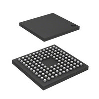
IC H8S/2214 MCU FLASH 112-TFBGA
Manufacturer
Renesas Electronics America
Series
H8® H8S/2200r
Datasheets
1.HS2214ECB62H.pdf
(938 pages)
2.HEWH8E10A.pdf
(19 pages)
3.D12312SVTE25V.pdf
(341 pages)
Specifications of DF2214BQ16V
Core Processor
H8S/2000
Core Size
16-Bit
Speed
16MHz
Connectivity
SCI
Peripherals
DMA, POR, PWM, WDT
Number Of I /o
72
Program Memory Size
128KB (128K x 8)
Program Memory Type
FLASH
Ram Size
12K x 8
Voltage - Supply (vcc/vdd)
2.7 V ~ 3.6 V
Data Converters
D/A 1x8b
Oscillator Type
Internal
Operating Temperature
-20°C ~ 75°C
Package / Case
112-TFBGA
For Use With
HS0005KCU11H - EMULATOR E10A-USB H8S(X),SH2(A)3DK2218 - DEV EVAL KIT H8S/2218
Lead Free Status / RoHS Status
Lead free / RoHS Compliant
Eeprom Size
-
Available stocks
Company
Part Number
Manufacturer
Quantity
Price
Company:

Part Number:
DF2214BQ16V
Manufacturer:
Renesas Electronics America
Quantity:
10 000


Section 6 Bus Controller....................................................................................119
6.1
6.2
6.3
6.4
6.5
6.6
6.7
6.8
Rev.4.00 Sep. 18, 2008 Page xxxiv of lx
REJ09B0189-0400
Overview............................................................................................................................ 119
6.1.1
6.1.2
6.1.3
6.1.4
Register Descriptions ......................................................................................................... 123
6.2.1
6.2.2
6.2.3
6.2.4
6.2.5
6.2.6
Overview of Bus Control ................................................................................................... 134
6.3.1
6.3.2
6.3.3
6.3.4
6.3.5
Basic Bus Interface ............................................................................................................ 139
6.4.1
6.4.2
6.4.3
6.4.4
6.4.5
Burst ROM Interface.......................................................................................................... 152
6.5.1
6.5.2
6.5.3
Idle Cycle........................................................................................................................... 155
6.6.1
6.6.2
Bus Release........................................................................................................................ 159
6.7.1
6.7.2
6.7.3
6.7.4
6.7.5
Bus Arbitration................................................................................................................... 162
6.8.1
Features................................................................................................................. 119
Block Diagram...................................................................................................... 120
Pin Configuration.................................................................................................. 121
Register Configuration.......................................................................................... 122
Bus Width Control Register (ABWCR)................................................................ 123
Access State Control Register (ASTCR) .............................................................. 124
Wait Control Registers H and L (WCRH, WCRL)............................................... 125
Bus Control Register H (BCRH) .......................................................................... 129
Bus Control Register L (BCRL) ........................................................................... 131
Pin Function Control Register (PFCR) ................................................................. 132
Area Divisions ...................................................................................................... 134
Bus Specifications................................................................................................. 135
Memory Interfaces................................................................................................ 136
Interface Specifications for Each Area ................................................................. 137
Chip Select Signals ............................................................................................... 138
Overview............................................................................................................... 139
Data Size and Data Alignment.............................................................................. 139
Valid Strobes......................................................................................................... 141
Basic Timing......................................................................................................... 142
Wait Control ......................................................................................................... 150
Overview............................................................................................................... 152
Basic Timing......................................................................................................... 152
Wait Control ......................................................................................................... 154
Operation .............................................................................................................. 155
Pin States in Idle Cycle ......................................................................................... 158
Overview............................................................................................................... 159
Operation .............................................................................................................. 159
Pin States in External Bus Released State............................................................. 160
Transition Timing ................................................................................................. 161
Usage Note............................................................................................................ 162
Overview............................................................................................................... 162
Related parts for DF2214BQ16V
Image
Part Number
Description
Manufacturer
Datasheet
Request
R

Part Number:
Description:
CONN SOCKET 2POS 7.92MM WHITE
Manufacturer:
Hirose Electric Co Ltd
Datasheet:

Part Number:
Description:
CONN SOCKET 4POS 7.92MM WHITE
Manufacturer:
Hirose Electric Co Ltd
Datasheet:

Part Number:
Description:
CONN SOCKET 5POS 7.92MM WHITE
Manufacturer:
Hirose Electric Co Ltd
Datasheet:

Part Number:
Description:
CONN SOCKET 3POS 7.92MM WHITE
Manufacturer:
Hirose Electric Co Ltd
Datasheet:
Part Number:
Description:
CONN SOCKET 5POS 7.92MM WHITE
Manufacturer:
Hirose Electric Co Ltd
Datasheet:

Part Number:
Description:
CONN SOCKET 2POS 7.92MM WHITE
Manufacturer:
Hirose Electric Co Ltd
Datasheet:
Part Number:
Description:
CONN SOCKET 3POS 7.92MM WHITE
Manufacturer:
Hirose Electric Co Ltd
Datasheet:
Part Number:
Description:
CONN SOCKET 4POS 7.92MM WHITE
Manufacturer:
Hirose Electric Co Ltd
Datasheet:

Part Number:
Description:
CONN HEADER 2POS 7.92MM R/A TIN
Manufacturer:
Hirose Electric Co Ltd
Datasheet:

Part Number:
Description:
CONN HEADER 4POS 7.92MM R/A TIN
Manufacturer:
Hirose Electric Co Ltd
Datasheet:

Part Number:
Description:
KIT STARTER FOR M16C/29
Manufacturer:
Renesas Electronics America
Datasheet:

Part Number:
Description:
KIT STARTER FOR R8C/2D
Manufacturer:
Renesas Electronics America
Datasheet:

Part Number:
Description:
R0K33062P STARTER KIT
Manufacturer:
Renesas Electronics America
Datasheet:

Part Number:
Description:
KIT STARTER FOR R8C/23 E8A
Manufacturer:
Renesas Electronics America
Datasheet:

Part Number:
Description:
KIT STARTER FOR R8C/25
Manufacturer:
Renesas Electronics America
Datasheet: